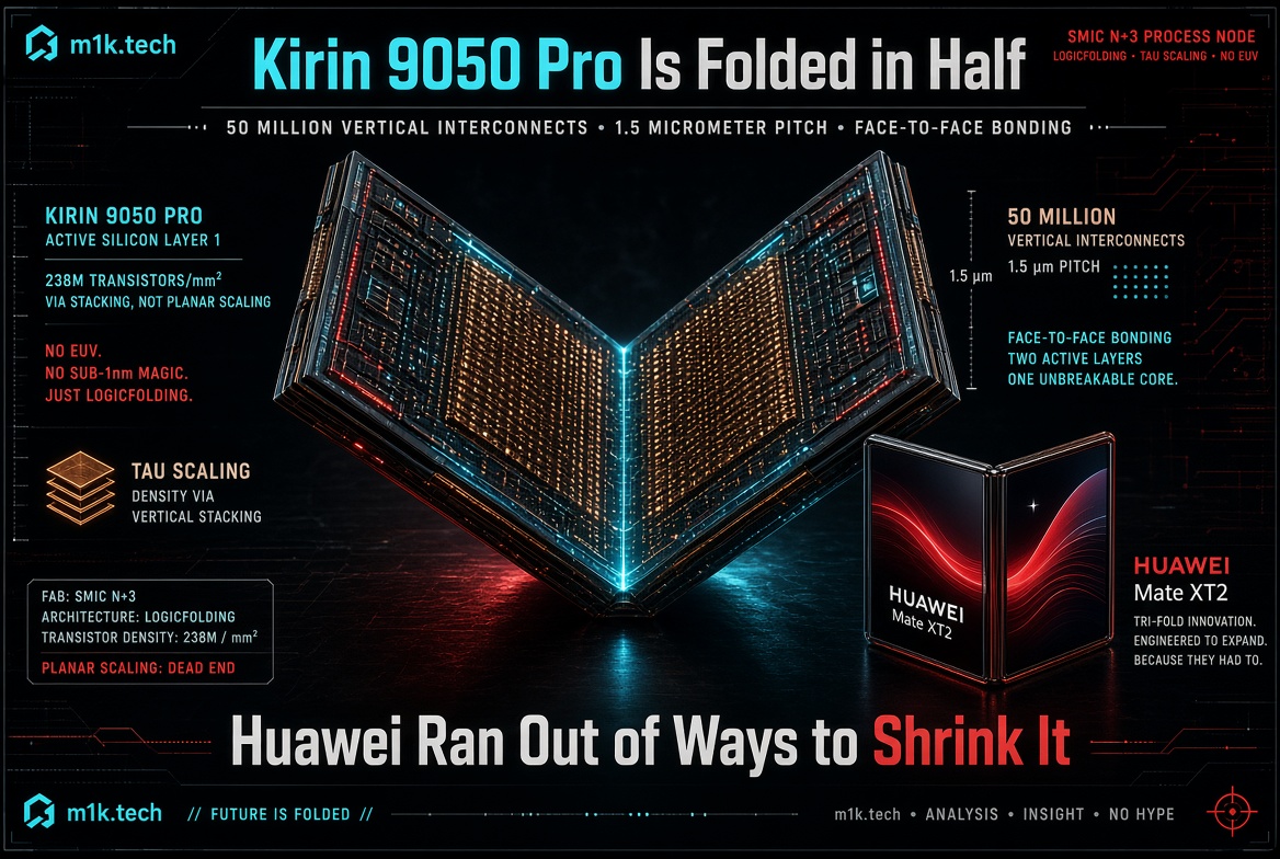
Fifty million vertical interconnects, spaced about 1.5 micrometers apart, bonding two active layers of silicon face to face so that a single CPU core lives on both floors at once. That is the physical claim sitting underneath every headline about Huawei beating export controls this week, and it is worth staring at for a second, because it is not a manufacturing claim. Nobody at SMIC printed a smaller transistor to make the Kirin 9050 Pro happen. Instead, Huawei folded the chip in half.
The launch itself was pure theater, and I mean that as a compliment. Huawei took the stage in Guangzhou on Monday with the Mate XT 2, its second tri-fold, starting at 19,999 yuan (roughly $2,980) for 16GB and 256GB, climbing to 29,999 yuan for the 2TB collector edition with the stylus kit. Sales open on 12 September. Xiaomi launched its own foldable hours later. Apple’s iPhone event lands Wednesday. Huawei already holds about 68 percent of Chinese foldable shipments and 22.6 percent of the Chinese smartphone market overall by IDC’s Q2 count, so this was never a phone Huawei needed to sell on merit alone. It was a slot on the calendar, claimed loudly.
What makes it interesting to me is that the chip inside is the first product to test a theory Huawei published four months ago and asked the industry to adopt.
What LogicFolding actually does to a die
He Tingbo, who runs Huawei’s semiconductor business and sits on its board, presented the Tau scaling law at IEEE ISCAS in Shanghai on 25 May, then followed it with a signed paper on the Chinese Academy of Sciences preprint server laying out the engineering. The pitch is that the industry should stop optimizing for space and start optimizing for time. Moore’s Law was only ever about time by proxy: smaller transistors mattered because they switch faster, denser wires mattered because signals travel less far. Huawei’s argument is that when you cannot shrink the transistor, you can still attack the delay, and the delay is what the user actually feels.
LogicFolding is the part of that theory you can hold in your hand. In a conventional SoC, logic gates sit on a plane and connect through metal layers stacked above them, and the performance ceiling is set by the critical path between flip-flop stages: how many gates the signal crosses, and how much resistance and capacitance the wire between them drags along. Past a certain complexity, the wire is the problem, not the transistor. LogicFolding splits the gates on that critical path across two vertically stacked active layers bonded at ultra-fine pitch, so the bond interface behaves like one more metal layer and cells can be placed across what used to be a die boundary. The two layers stop being two dies and start behaving like one continuous layout substrate.
Huawei’s own paper is specific about what that costs. The gear ratio between hybrid-bonding pitch and top-metal pitch has to stay below three and ideally near one, which, with a top-metal pitch around 720nm means bonding pitch below 2 micrometers; the Kirin implementation lands at 1.5. Alignment accuracy has to hold under 0.5 micrometers, TSV pitch under 6, failure rate below 100 parts per million, with intelligent redundancy pushing the repair rate to 99.9 percent so yield can approach something economically sane. Around 10 to 15 percent of those 50 million vertical connections carry high-speed signal rather than power or ground.
The results Huawei claims from that are the most concrete numbers in the whole story. Transistor density on the folded chip goes from 155 to 238 million transistors per square millimeter in a single generation, which by Huawei’s own reckoning would previously have taken roughly three years of geometric scaling. The performance core gains 41 percent in power efficiency and nearly 13 percent in maximum frequency. A global network-on-chip datapath built across both layers cut its area by 55 percent. SRAM is where I find it most convincing: access speed and energy per bit depend heavily on bitline and wordline length, and shortening those pushed SRAM operating frequency up more than 40 percent. Inside a representative core, clock buffers dropped by more than half, clock skew fell 25 percent, and total wiring length came down about 30 percent.
The launch version of this is more modest than the theory allows. Folding is applied selectively to critical paths, not the whole design. TSV landing has only moved one step below top metal, when the roadmap wants it down at M6 to free more than 30 percent of upper-level routing. The stack is two layers, not four. Huawei is being conservative on its first commercial attempt, which is the right instinct when your yield story is what everyone is waiting to attack.
The node underneath, and why it stopped mattering as much
Huawei did not announce a process node for the Kirin 9050 Pro, and that omission is deliberate, not coy. The predecessor tells you most of what you need. SemiAnalysis tore down the Kirin 9030 Pro in June and found SMIC’s third-generation 7nm process, N+3, with a minimum M0 metal pitch of 32.5nm. That is tighter than the 36nm pitch Intel ships in Panther Lake on 18A, a fact that got recycled into a lot of triumphant headlines and one very careful caveat from the lab that measured it: M0 is a local intra-cell routing layer, and one cherry-picked dimension is not a process.
The full picture is more interesting than the headline. N+3 reaches 113.4 million transistors per square millimeter on a normalized basis, slightly ahead of TSMC’s N6 at 107.7, with no EUV anywhere in the flow. SMIC gets there by pulling every design-technology co-optimization lever available at once: fin depopulation down to two fins per transistor, contact over active gate (which TSMC’s N6 does not use), single diffusion breaks, a 228nm cell height, a 57nm contacted gate pitch, and a 3:2 M1-to-gate ratio that buys local routing flexibility at the price of layout complexity. The M0 pitch is below what a single deep-ultraviolet spacer step can resolve, so SMIC cascades a second one, self-aligned quadruple patterning, and you can see the bill in the cross-section: the M0 trenches come out visibly re-entrant, narrower at the bottom than the top, at a higher aspect ratio than the layers above them.
Every one of those choices adds masks, overlay sensitivity, cost and yield risk. That is the whole export-control effect in one sentence. The controls did not stop China from reaching N6-class density. They made it expensive and fragile, and the American Enterprise Institute’s April report put SMIC’s 5nm-class yields around 20 percent, which is the kind of number that works for a halo phone and not for shipping AI accelerators by the million.
And the density does not convert. The Kirin 9030 Pro’s prime core sits roughly at Cortex-X2 territory per clock, a 2021 design, and Apple’s efficiency core delivers about 20 percent more integer performance at 1W than Huawei’s prime core does at 4.5W. Both the middle and tiny cores failed to hold their rated maximum frequencies in testing, which points at thermal or power limits rather than design ambition. That is the gap LogicFolding exists to attack, because the planar road ahead is ugly: a hypothetical N+4 would need a shorter cell, another layer pushed into quadruple patterning and a tighter gate pitch just to land near TSMC N5, and an N+5 would need backside contacts and a wholesale integration shift to reach Intel 18A density at far higher cost. I wrote back in July about China building its own immersion DUV steppers, five machines this year and twenty next, and the domestic EUV programs behind that are still a light-source problem: the LDP prototypes are putting out 100 to 150 watts against the 250 watts a commercial tool needs, and the 600 watts ASML actually ships. Nobody is rescuing SMIC with a domestic scanner before this phone is discontinued.
The chip Huawei actually shipped
The CPU is a nine-core Linxi arrangement plus a tenth always-on micro core, and the split is unusually granular: one super core, two big cores, four efficiency cores, two small cores, with the micro core handling always-on display, sensor hub and notification polling on its own power island. Peak frequency is 3.1GHz, exactly the figure on He Tingbo’s May roadmap for 2026, with 3.39GHz penciled for 2027, 3.71GHz for 2028, past 4GHz in 2029 and around 5GHz by 2031. Huawei claims 24 percent higher peak single-core and 52 percent better multi-core concurrency against the Kirin 9030 Pro, plus 50 percent faster large-file loading.
The GPU got the biggest share of the silicon budget. Maleoon doubles both compute units and L2 cache, and Huawei quotes a 142 percent jump in real-time rendering, hardware ray tracing rated at up to 50 million rays per second, and 4 K video export that’s more than 40 percent faster. On the NPU side, the DaVinci block runs a 30-billion-parameter multimodal mixture-of-experts model locally with about 2 billion parameters active per pass, Huawei’s own Pangu 30B-A2B, which, as far as I can tell, is the first time anyone has claimed an on-device MoE multimodal model at that scale in a phone. The Balong modem carries Tiantong satellite calling and BeiDou messaging with a 42 percent better satellite paging success rate and 25 percent lower weak-signal latency in basements and on high-speed rail. The security block pairs a mobile security processor with an embedded secure element at EAL5+ and adds hardware detection for post-quantum algorithms, which lands about three weeks after Google put post-quantum crypto into the Pixel 11’s boot ROM and suggests everyone’s 2027 silicon is going to have a PQC bullet point whether or not the threat model justifies it yet.
Independent numbers are thin, and that’s where I get annoyed. The only benchmark anyone has is a leaked Geekbench 6 single-core score of 2,084 at 3.1GHz, attributed to the chip by Digital Chat Station on 4 September, with no matching public entry in the Geekbench browser and no confirmation that the silicon tested was even this part. Take it at face value, and it is about 12 percent up on the Kirin 9030 Pro, against roughly 3,582 for Apple’s A18 Pro and around 3,155 for Snapdragon 8 Elite. Huawei’s own 42 percent headline is measured against the previous Mate XT, not against anything Qualcomm or Apple sells. A company that controls its own benchmarks, its own foundry relationship, and its own operating system is grading every part of its own homework here, and the 55 percent density figure has not been independently verified by anyone with an electron microscope. It will be, within a couple of months, and I would rather wait for that than repeat the press release with more adjectives.
Why the density claim needs an asterisk
Here is the sleight of hand that bothers me most, and it is accounting rather than fraud. When Huawei says its high-end chips will reach 1.4nm-equivalent transistor density by 2031, it is measuring transistors per package footprint, not per patterned die. Stack a second active layer, and your density roughly doubles without a single improvement in lithography. Apply that same methodology to something like AMD’s MI450X, an N2 top die on an N3P base, and you get a theoretical 460 million transistors per square millimeter in 2026 against Huawei’s projected 295 in 2031. Huawei’s roadmap targets 215 MTr/mm2 by 2030 and then jumps to 295 in 2031, which implies either a third active layer, some partial EUV insertion, or planar DUV scaling more aggressive than anything SMIC has demonstrated.
None of which makes LogicFolding fake. Stacking active logic across a fine-pitch bond and splitting a critical path across tiers is harder than what AMD does with V-Cache or by placing active interposer dies under compute dies, because those move cache and I/O rather than pieces of the same logic block. The technique is real, and the frequency and SRAM gains are the proof, not the density number. But “1.4nm equivalent” is a marketing unit, and the fact that it maps onto a foundry node name that Huawei will not be manufacturing at is the entire point of choosing it. I have argued before that the moat in AI hardware keeps relocating from the transistor to the packaging line, and Huawei is the first company to build a public scaling law on top of that relocation.
The phone is not the point
Huawei says it has mass-produced 381 chips over six years using this framework, which reframes the Kirin as a validation vehicle rather than a flagship. Mobile is the hard test case: a phone SoC cannot hide a bottleneck behind cluster interconnect; all the perceived performance has to come out of one die inside a few watts. Prove it there, and you can take it somewhere that matters more.
That somewhere is the Ascend line. The same paper lays out an AI system path built on three pieces: a Unified Bus that collapses the PCIe/NVLink/Ethernet protocol stack into one peer-to-peer memory-semantic fabric and claims to cut remote access latency from tens of microseconds to around 100 nanoseconds, a near-package optical engine called Hi-ONE running 8Tb/s per module to get past what copper can do above a few terabits, and 3D Folding aimed at what Huawei calls the fan-out dilemma. That last one is the document’s sharpest observation. In a 2.5D AI package, compute scales with die area, so N squared, while memory bandwidth, I/O, and power delivery all enter through the die edge, so N. Compute grows quadratically, and everything feeding it grows linearly, which is why better logic nodes stop rescuing the design. Move power delivery to the backside, memory onto hybrid bonds, and I/O into near-package optics, and those resources scale with surface instead of perimeter. Ascend 950 this year and Ascend 990 next use chiplets and conventional 3D stacking; LogicFolding proper is slated for Ascend around 2030.
Whether any of that survives contact with 20 percent yields is the open question. But the strategic direction is unambiguous, and it lines up with something I have written about repeatedly: HiSilicon was supposed to die in 2020 and instead became the backbone of China’s AI stack. Huawei spent 121.38 billion yuan on R&D in the first half of 2026, more than a quarter of revenue, and it is spending it on the parts of the stack export controls cannot reach.
The diffusion matters more than the chip. SMIC is licensing N+2 and N+3 to Hua Hong at the government’s direction rather than by commercial choice, which turns a single sanctionable fab into an ecosystem. Researchers at Peking University have a prototype EDA tool specifically for LogicFolding’s multilayer floorplanning, because the Western toolchain has no flow for splitting a logic block across bonded tiers, and Huawei has been locked out of Synopsys and Cadence since 2020 regardless. Memory is the one dependency Huawei hasn’t solved: the Kirin 9030 Pro shipped with Samsung LPDDR5X on a 1a node in some variants and CXMT parts in others, and Richard Yu openly grumbled on stage about memory component costs squeezing this launch. That is the same wave I covered when memory pricing pushed every Samsung foldable up $100, except Huawei is absorbing it at 20,000 yuan with a domestic supply chain that is still catching up on DRAM.
What I think it means
Xiaomi’s foldable landing the same afternoon on the Xring O3, which drops efficiency cores entirely and leans on hybrid bonding, is not a coincidence either. Two Chinese phone makers, one launch day, both reaching past the process node into packaging and architecture for gains they cannot buy from a foundry. When I wrote about China’s integrated circuit export numbers and what 88.7 percent growth actually measured, I concluded the headline overstated capability and understated direction. Same read here. Meanwhile Qualcomm spent those same years building the one edge-silicon business the export regime cannot really touch, which is the mirror image of Huawei’s problem: when you cannot route around the chokepoint commercially, you route around it physically.
Export controls were designed on the assumption that the node is the chokepoint. Huawei’s answer is to make the node one input among several, and to argue publicly that the industry’s scoreboard should change accordingly. That argument is self-serving, and it also happens to be where TSMC, Intel, and Samsung are all heading anyway, which is why TSMC’s own A14 plans to skip the $380 million lithography tool that was supposed to be mandatory at that node. Everyone is discovering the same physics. Huawei just got there under duress and needed a name for it.
The thing I cannot resolve is yield. Every claim in this piece rests on wafer-to-wafer hybrid bonding at 1.5 micrometers holding together across millions of units at a failure rate under 100ppm, on a process that already burns extra masks to reach density, but barely converts into performance. Wafer-to-wafer bonding means a defect on either layer kills both. If that works at volume, the 2031 roadmap is a real threat and the export-control framework is aiming at the wrong organ. If it does not, the Mate XT 2 is a 20,000-yuan technology demonstration with a great story attached, and we will find that out from a teardown lab in Oregon long before we find it out from Huawei. Ask me again when the Mate 90 ships this chip in volume.
Sources
- Huawei, HUAWEI Presents the Tau Scaling Law, IEEE ISCAS keynote, May 25, 2026
- SemiAnalysis, Is SMIC N+3’s Metal Pitch Smaller than Intel 18A’s?, STEEL teardown of the Kirin 9030 Pro, June 14, 2026
- TechInsights, SMIC N+3 Confirmed: Kirin 9030 Analysis Reveals How Close SMIC Is to 5nm
- Leon Liao, Huawei Unveils Tau Scaling Law, analysis of He Tingbo’s ChinaXiv paper, May 25, 2026
- Caixin Global, In Depth: Huawei’s Bid to Rewrite the Rules of Chip Scaling, June 2, 2026
- Reuters, Huawei launches new foldable smartphone as competition with Xiaomi, Apple heats up, September 7, 2026
- KAD, Huawei Kirin 9050 Pro Brings 3D LogicFolding to Mate XT2, September 7, 2026
- GizmoChina, Huawei Mate XT 2 tri-fold launches with new Kirin 9050 Pro and Lingdun privacy screen, September 7, 2026
- TechTimes, Huawei Kirin 9050 Pro Launches: LogicFolding Moves From Roadmap to Silicon, September 7, 2026
- Global Times, Huawei unveils high-performance Kirin 9050 Pro chip, September 7, 2026
- The Diplomat, China’s EUV Lithography Progress: Parsing Signal From Noise, July 8, 2026
- Tom’s Hardware, China begins mass production of homegrown immersion chipmaking machines, July 2026