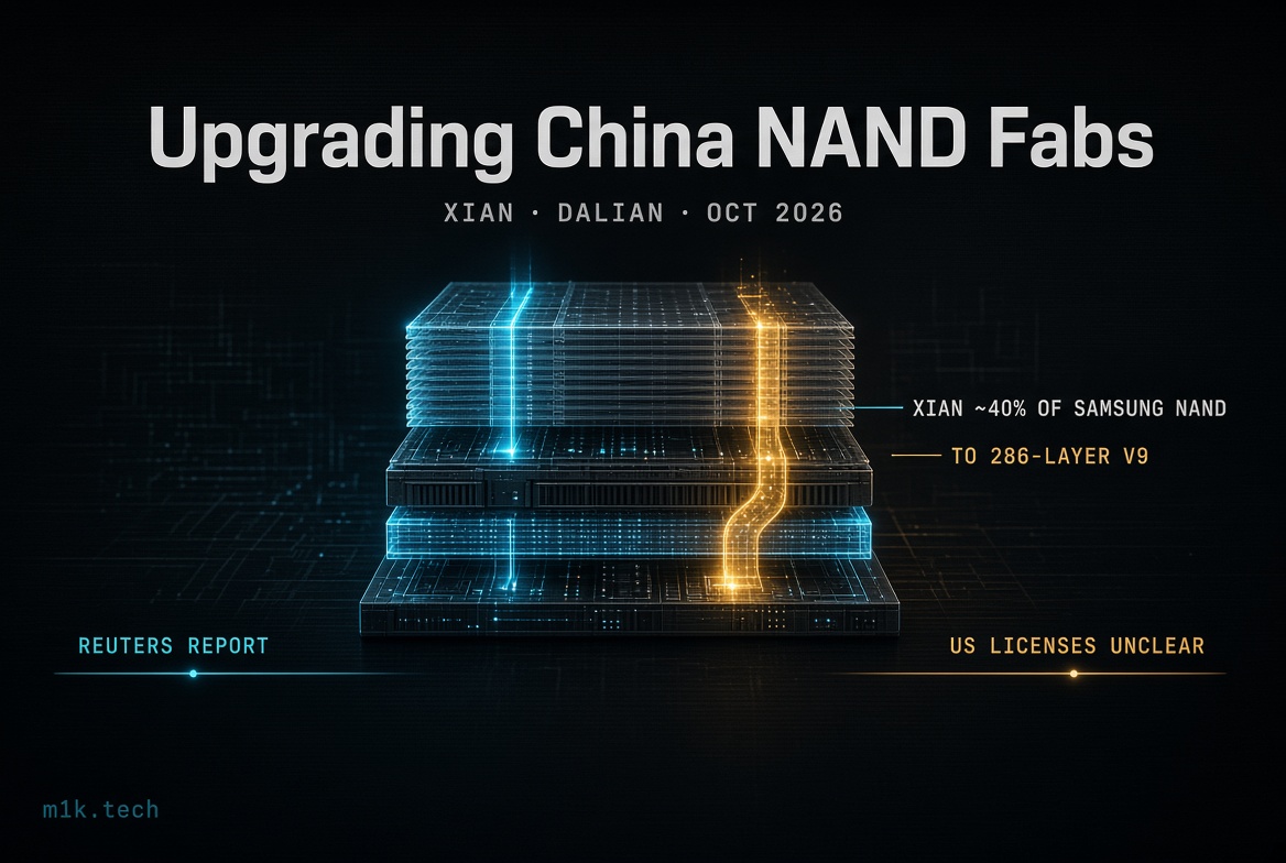
Samsung and SK Hynix are upgrading their NAND factories in China, four people familiar with the plans told Reuters, and the Xian plant alone makes about 40% of Samsung’s NAND output. It currently turns out chips of roughly 200 layers.
Under an internal project called Monami, according to one source, Samsung is converting Xian to its 286-layer V9 NAND, aiming for 5,000 wafers a month in December and 40,000 by December 2027. SK Hynix wants to move Dalian from 192 layers to 240 or more, and one person says it may ask Washington for permission to do research on 300-plus layers there. Samsung told Reuters the work complies with US export rules and that it is not expanding capacity or building new facilities. A ramp from 5,000 to 40,000 wafers a month on a converted line may or may not count as expansion, depending on a baseline the report doesn’t give, and I can’t settle that from here.
The legal footing is the part that matters. Both companies need US licenses every year to install American-made tools such as etchers in China, and the Commerce Department’s export bureau said in 2025 that it intended to license existing operations but not capacity expansion or technology upgrades. Reuters could not determine how much of the equipment for these upgrades has actually been approved, and the bureau didn’t answer directly. Both companies say they are working closely with Washington. Dalian is also the only NAND fab of Solidigm, the former Intel business now preparing a US IPO, so that plant carries more than SK Hynix’s own output. I covered the two testing Chinese etching tools in August, a story Samsung denied, and the tool question is what decides whether any of this happens.
Standing still has been costing them.
.
Sources
- Reuters via CNBC: Samsung, SK Hynix upgrading China plants to make more advanced chips, people say, 21 October 2026