Digital infrastructure already eats somewhere between 6 and 12 percent of the world’s electricity, and that number climbs every time another AI cluster comes online. Superconductors carry current with zero resistance, which makes them one of the very few physical mechanisms, alongside things like ultrafast antiferromagnetic switching, that can actually bend that curve rather than shave a few points off it. The catch has always been the cooling. Every useful superconductor demands extreme cold, and the materials that look most promising for warmer operation, the copper-oxide cuprates, have a reputation for resisting every conventional attempt to improve them. A team at Chalmers University of Technology in Sweden published a result earlier this year in Nature Communications that sidesteps the usual playbook: they left the chemistry of the superconductor alone and instead reshaped the surface beneath it. The numbers they got back are hard to wave away.
YBa₂Cu₃O₇−δ, which everyone calls YBCO, has been picked over since the late 1980s. Its superconductivity lives in stacked copper-oxygen sheets, the CuO₂ planes, where electrons pair into Cooper pairs and glide through the lattice without scattering. Two of the figures that matter most, the transition temperature Tc and the upper critical magnetic field Hc,2, are both held down by competing electronic orders. The worst offender is the charge density wave, or CDW, which poaches the very electrons that should be forming Cooper pairs.
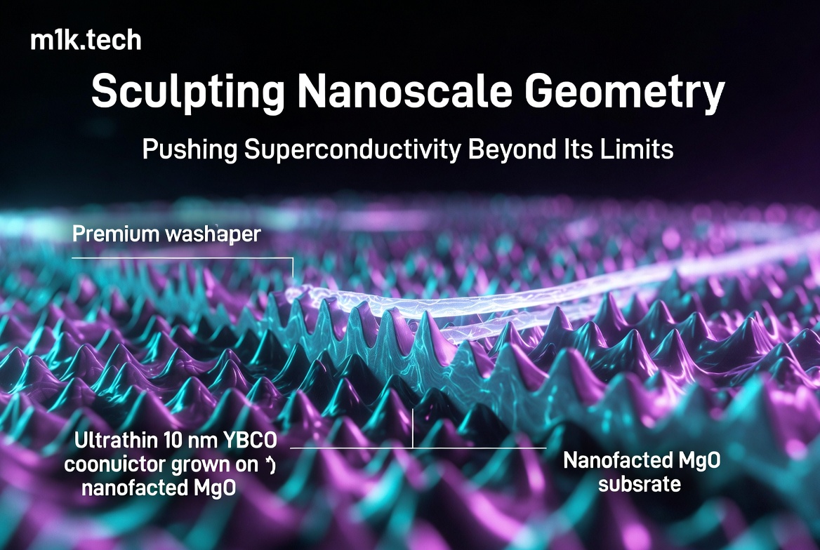
Floriana Lombardi’s group in the Department of Microtechnology and Nanoscience attacked the geometry rather than the recipe. Before depositing any YBCO, they annealed (110)-oriented magnesium oxide substrates at 790°C in vacuum, and the MgO surface responded by self-organizing into a regular washboard of nanoscale triangular ridges and valleys, each about 1 nm tall and 20 to 50 nm wide. Grow a YBCO film on top at 10 nm thickness, less than a millionth the width of a human hair, and the lattice sits close enough to the sculpted substrate that the geometric potential of the ridges starts dictating how the CuO₂ planes arrange themselves electronically.
The payoff is steep. Set the 10 nm films on nanofaceted MgO against 50 nm films grown on ordinary flat substrates and the onset temperature jumps by more than 15 K, with the upper critical field climbing more than 50 Tesla higher. For a field where chemical doping tweaks buy you a few kelvin if you are lucky, those are not marginal gains.
Two coupled phenomena drive it: electronic nematicity and the direction in which the charge density wave runs. In bulk YBCO crystals and thick films, the CDW is bidirectional, ordering along both the a-axis and the b-axis simultaneously, and this two-way competition suppresses superconductivity. On the nanofaceted substrate, the interfacial potential V_eff imposed by the surface geometry snaps that symmetry, and the CDW goes unidirectional, locked to the b-axis alone. Annica M. Black-Schaffer at Uppsala and Götz Seibold at BTU Cottbus-Senftenberg developed the theoretical model, which points to something more interesting than reduced competition. The unidirectional CDW actively cooperates with superconductivity, strengthening the effective pairing interaction through a coupling between the nematic order and the superconducting condensate. An electronic order that normally fights superconductivity flips to its side once its geometry is pinned down.
That cooperation depends sharply on thickness, and that is where the whole thing becomes a nightmare to manufacture. V_eff gets screened by the film’s own electronic structure, so in a 50 nm film, the bulk of the material sits too far from the substrate, and the geometric signal washes out before it can do anything. Only in the ultrathin regime, with 10 nm being the sweet spot the experiment landed on, does V_eff stay strong enough to reorganize the CDW. That bakes in a hard tension. Ultrathin films are fragile and awkward to pattern lithographically, and they pick up contamination and disorder faster than you can characterize them. Getting 10 nm YBCO into a real device means solving a stack of problems the physics paper never set out to touch.
The deeper result is that substrate geometry now counts as an independent knob for tuning cuprate superconductivity. Almost every prior attempt to improve YBCO has gone through chemistry: nudge the oxygen stoichiometry, or substitute atoms into the barium or copper sites to retune the doping of the CuO₂ planes. Those moves are hard to control precisely and impossible to undo once the film exists. Sculpting the substrate occurs before deposition and repeats cleanly during standard vacuum annealing, without ever affecting the superconductor’s intrinsic chemistry. In materials-engineering terms, it is a processing step rather than a compositional change, and processing steps tend to scale to industry far more gracefully.
The paper, “Boosting superconductivity in ultrathin YBa₂Cu₃O₇−δ films via nanofaceted substrates,” is at https://www.nature.com/articles/s41467-025-67500-2, and the Chalmers press release sits at https://www.chalmers.se/en/current/news/mc2-superconductor-advance-could-unlock-ultra-energy-efficient-electronics/.
Nobody on the team is pretending this is a route to room-temperature superconductivity. A 15 K gain is real money, but YBCO still has to run somewhere around −180 to −196°C, and room temperature sits another 200 K or so up the ladder. What the work proves is a design principle: the nanoscale geometry of an interface can rearrange the competing electronic orders within a cuprate so that they help rather than hinder. The one thing worth doubting is whether that principle survives contact with other cuprate compositions. Confined to YBCO, it stays a footnote in the literature. The real prize is portability: if the same washboard geometry reorganizes the electronic orders in other cuprates, the result stops being a single clever measurement and turns into a general way to engineer superconductors. That is what the next paper has to answer.