Press a wafer face-down against a rotating pad flooded with abrasive slurry, and the combination of mechanical grinding and chemical dissolution shaves material off the surface until it’s flat to sub-nanometer roughness. That’s chemical mechanical planarization, and it sounds simple right up until you look at what “controlled” has to mean. IBM commercialized it around 1990 at its Burlington, Vermont fab, solving a problem that had turned brutal as the industry stacked up multilevel metal interconnects: deposit conductor layers over existing circuit topography and you build hills and valleys that optical lithography cannot hold in focus. CMP flattens those layers globally, not just in local patches, and that global flatness is what made deep submicron logic possible in the first place.
By the mid-1990s Applied Materials had shipped the Mirra platform, which anchored the market for a generation. Push to sub-7nm logic today and a single chip can demand 20 to 30 discrete CMP steps across dielectric, metal, and barrier layers. Even at the mature nodes that carry power electronics, MEMS, and sensors, you’re looking at 3 to 8 steps per device. Every one removes a controlled thickness, and that word is carrying an enormous load. Remove too little and the surface won’t take the next deposition cleanly; remove too much and you’ve thinned a functional layer past spec, or punched clean through into the layer beneath. The window is narrow, it drifts as the pad wears and the slurry ages, and it varies across the face of the wafer.
Metrology and CMP have always been the same problem wearing two hats. The real question is how tightly you bolt them together, and that’s precisely what Hwatsing’s new system goes after.
The old flow keeps them apart. Polish the wafer, unload it, walk it to a standalone metrology tool (an optical reflectometer, an ellipsometer, a four-point probe), measure the film thickness, then feed that number back into the recipe for the next wafer or lot. The round trip burns time, eats monitor wafers, and drops in a lag long enough to miss within-lot drift entirely. If your pad is degrading over the course of a 25-wafer cassette, you might not find out until the damage is baked in.
Endpoint detection was the first real attempt to close that loop, arriving commercially in the mid-1990s. Instead of measuring after the fact, it catches the moment the target layer is reached mid-polish. Optical interferometry does it through a small window in the pad; motor-current sensing does it by reading the friction change as the tool crosses from one material into another. Applied Materials’ ISRM and Lam Research’s optical endpoint systems were the early commercial versions, both in-situ, measuring with the wafer still on the platen. The catch is that endpoint tells you when to stop. It won’t hand you a precise film-thickness map before you begin, and confirming the result afterward still usually means a separate measurement.
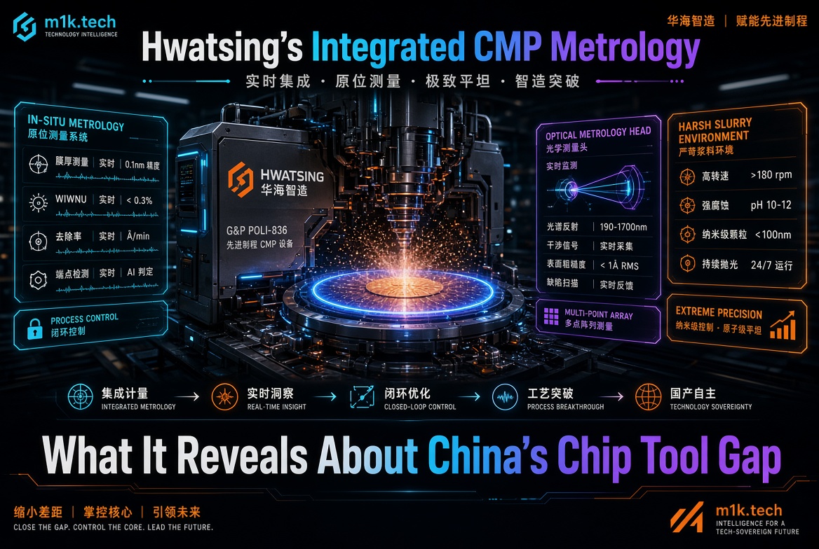
Integrated metrology squeezes the loop tighter still. The measurement stations physically attach to the CMP tool itself, one upstream of the polish module and one downstream, and wafers roll through them during the robotic transfers that already happen anyway. No separate queue, no context switch, no cleanroom hop that invites its own contamination. The data drops straight into the process controller. Therma-Wave and ADE (later absorbed into KLA) were building this architecture in the early 2000s, and it’s since become standard on leading-edge CMP platforms from Applied Materials and Lam.
Hwatsing Technology has spent a decade in this business. It spun deliberately out of Tsinghua University’s State Key Laboratory of Tribology in 2013, backed by Tianjin municipal co-funding, and its Universal-300 and Universal-300 Dual platforms already run 300mm wafers in production at domestic Chinese fabs. The new product goes the other direction on wafer size: a six-inch, 150mm system with pre- and post-polish film-thickness measurement built into the tool body.
Patent CN116551554B lays out the architecture, filed May 2023 and granted July 2026, a timeline that lines up almost to the month with the product announcement. The IPC classifications read like a description of the concept itself: B24B37/00 for CMP machines, B24B49/00 for measuring during machining, B24B51/00 for automatic control, B24B57/02 for slurry feed to the grinding zone. Measurement is part of the machine, not a bolt-on. Optical probe reflectometry reads film thickness at the pre-measurement station before the wafer hits the platen, then again downstream after polishing, with the transfer arm carrying it through both stations as part of normal handling. The pre-measurement sets a baseline; the post-measurement confirms the result and, the part that actually matters, feeds back to tune the recipe for the wafers still coming.
Hwatsing names the first customer only as a leading domestic optical silicon materials producer. “Optical silicon” most likely means wafer production for photonic applications, waveguides and photodetectors and silicon photonics interposers, where post-polish surface uniformity dictates optical loss and coupling efficiency directly. It might instead mean solar-grade silicon, where CMP shows up in some high-efficiency cell designs. Either reading lands in the same place: film-thickness uniformity across the wafer face is the primary quality metric, which turns integrated metrology from a luxury into the point.
Six inches as the launch platform is a legible bet. That size is still the production standard for silicon carbide power devices, compound semiconductors like GaAs and GaN, and a big slice of silicon MEMS and sensor work, which happen to be exactly the parts China’s EV industry leans on hardest, with industrial automation and the telecom buildout close behind. SiC is the sharp edge here. It’s harder than silicon, so CMP removal rates run low, and surface quality demands are punishing because SiC defects propagate up into the epitaxial layers and drag down device breakdown voltage. Getting CMP metrology right on six-inch SiC is not a warm-up exercise.
Eight- and twelve-inch integrated metrology is a much harder build. More wafer area means more within-wafer non-uniformity to characterize, tighter spatial resolution on the measurement system, and stiffer demands on robotic handling to place the wafer reproducibly under the probe. Starting at six inches is a real engineering call rather than a shortfall to apologize for, and it draws a firm line around what’s actually been demonstrated.
Hwatsing’s commercial run in CMP equipment is remarkable by any honest reading. The company held roughly 1% of the China CMP equipment market in 2018. By 2025, per Bernstein and Soochow Securities data cited in the South China Morning Post, it had 85% of the domestic-supplier segment and 37% of the all-competitor China market. Seven years from a rounding error to dominant in a single equipment category, driven in large part by export controls that put Western CMP tools out of easy reach and pushed domestic fabs to qualify alternatives.
The same numbers expose the asymmetry. Domestic suppliers hold about 39% of China’s wafer-fab polishing equipment market, a real win. Domestic self-sufficiency in metrology and inspection overall sits near 10%. That gap is the whole story. CMP without reliable closed-loop metrology is open-loop control in every sense that matters: you polish to a time recipe and hope the result lands in spec instead of measuring your way to a confirmed one. The 10% figure says KLA and Onto Innovation (the 2019 Nanometrics/Rudolph merger) are still wired deep into Chinese fabs even after CMP hardware got substantially swapped out.
Building the measurement into its own tools is Hwatsing’s answer to that gap. If you can’t freely buy a KLA Spectra or an Onto Innovation Atlas standalone, folding measurement into the CMP platform keeps the closed loop intact without a second procurement fight. What’s still unsettled is whether captive metrology built to serve one vendor’s polisher can hit the same marks as best-in-class standalone inspection. Standalone tools have historically owned the advantage in measurement accuracy, spatial resolution, and the ability to catch far more than film thickness: particles, scratches, micro-roughness, crystallographic damage. A pre/post reflectometry station tuned for the thickness feedback loop is not a full wafer inspection system, and it was never trying to be.
The stakes climb as nodes shrink. At the mature nodes this six-inch tool serves, the process windows are wide and the defect budgets forgiving, and integrated reflectometry may well be enough for production control. At leading-edge logic, where CMP has to hold sub-angstrom surface roughness and defect density targets fall to single digits per square centimeter, the metrology bar is a different animal entirely.
Hwatsing’s origins are worth sitting with, because they show both the reach and the ceiling of China’s state-directed equipment strategy. The company was engineered into existence: Tianjin money, a Tsinghua research base, tribology expertise from a State Key Laboratory, all aimed at commercializing CMP work born in academia. The patent prosecution timeline tracks the product announcement so closely it reads as a filing meant to fence off a specific design already deep in development. Lab research becomes a spinout, the spinout ships a product, the product lands at a domestic customer. The machine ran exactly as designed.
The doubt is about what that machine actually optimizes for. Hwatsing’s share ballooned during a stretch of tightening export restrictions, which means the competition it beat was being pulled off the field precisely as its numbers climbed. Applied Materials, Lam, and their metrology partners weren’t fighting at full strength in China through those years. Benchmark the Universal-300 against an Applied Materials Reflexion Impulse on within-wafer non-uniformity, throughput, and advanced-node defect density, and you’ll find those numbers aren’t public, which tells you something on its own.
That doesn’t shrink the accomplishment. Building a working integrated CMP metrology system out of domestic parts is real engineering: the optical probe, the robotic transfer integration, and the live feedback loop are not casual implementations, and the patent claims describe a specific mechanical and optical architecture that took actual work to reduce to practice. Hwatsing’s engineers, a lot of them out of Tsinghua tribology, built a thing that works well enough to ship into production.
Two facts have to sit in the same hand: this is a meaningful move in China’s non-lithography tool buildout, and it’s a six-inch system aimed at mature nodes while the frontier of process-control metrology runs at 300mm with angstrom-level sensitivity. That last comparison is where the doubt should land. The frontier isn’t waiting at six inches, and the distance to it is the hardest thing Hwatsing has yet to build across.