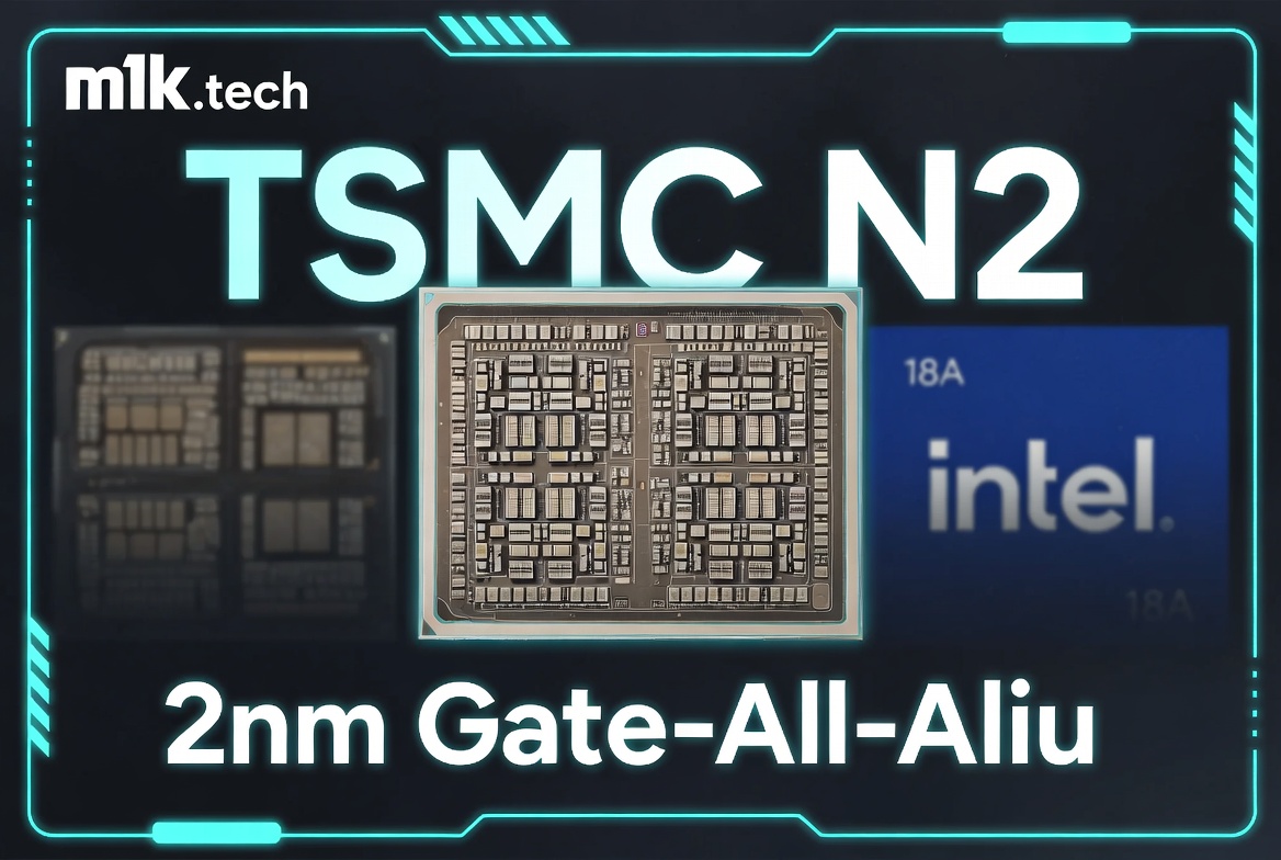
TSMC is ramping its 2nm node into volume this half, and for the first time since 2015 the transistor inside it is not a fin. N2 is gate-all-around, the nanosheet design that stacks the channel into horizontal sheets the gate wraps on every side, and it is the change N3 deliberately deferred. Samsung jumped to nanosheets three years ago and never turned them into a real business. TSMC let Samsung eat the early defect rates and stayed on proven FinFET through N3, shipping the new transistor only now, with the customer list already locked. That lateness is the strategy, the same one it has run since 28nm, and it keeps working.
A FinFET wraps the gate around three sides of the channel, and at N2 dimensions three sides can no longer stop the thing leaking current when it is supposed to be off. Nanosheets wrap the gate on all four, stacking two or three horizontal sheets where a single fin used to stand, which hands back the electrostatic control the fin was bleeding away and lets a designer tune drive current by changing sheet width, something fins never allowed. That is the performance-and-power step 5nm and 3nm kept delivering in smaller and smaller slices. The first new transistor in a decade, and the whole industry has bet the next ten years on it yielding.
Intel’s 18A is ramping the same year, also gate-all-around, and it carries something N2 does not: backside power delivery, the power rails routed underneath the transistors instead of fighting them for room up top. That is a genuine architectural edge, and Intel is leaning on it hard to claim it has leapfrogged TSMC for the first time in a decade. TSMC’s counter is to hold its own backside-power node back for next year and bet that 18A’s real-world yield is nowhere near what Intel’s slides say. For one node, after thirty years, the lazy assumption that TSMC just has the best process is an open question again.
The chatbot hype of late 2022 turned into the largest capital-spending wave in computing history, and it answered the demand question N3 left open: the leading edge now exists for AI. The giant datacenter accelerators that train and run these models are the most important customers at the front of the line now, ahead of phones, and N2 is being built for them as much as for the next iPhone. The binding constraint is not even the transistor anymore. It is advanced packaging, the ability to stitch these enormous dies and their stacks of memory into one working part, and that has become its own bottleneck sitting right beside the node.
An N2 wafer reportedly runs around thirty thousand dollars. At that price the list of organizations that can tape out a chip here has collapsed to a dozen or so trillion-dollar companies and AI labs, the only ones that can spread the cost across enormous volume or simply eat it on enormous funding. The fabless model started life as a promise that anyone with a good design could rent world-class manufacturing, and that promise has now fully inverted: the leading edge is the most exclusive industrial process on the planet, open to maybe a dozen buyers and gated by a single company in one country. Everyone else builds on a node that is years behind, and for the overwhelming majority of chips that is completely fine. For the handful that genuinely need the front of the line, the door is shut unless you are one of the dozen.
The single-island risk that has hung over every advanced node for a decade is finally getting a partial answer. TSMC is pouring tens of billions into fabs in Arizona, with more going up in Japan and Germany, building real leading-edge capacity off Taiwan for the first time. A fab in Arizona runs slower and costs more than the same fab in Hsinchu, and the single most advanced node still stays home for now. But the concentration that made TSMC both indispensable and terrifying is, slowly and under heavy political pressure, starting to spread. The customers footing the bill would have preferred never to learn why they needed it spread.
For fifteen years the easy story held: TSMC had the best transistor and everyone else chased it. This year complicates it. The company changed the transistor on schedule, held onto its customers, and ramped gate-all-around the way it has ramped every node since 28nm, quietly and into volume while rivals were still issuing press releases. That much is the old, reliable TSMC. What is new is that Intel finally has a credible node with a power trick TSMC cannot answer until next year. The wafer cost has climbed to a number that locks out everyone but a dozen giants. And the fabs that matter are, grudgingly and a decade late, starting to leave the island. TSMC still has the lead. What it no longer has is the luxury of treating that lead as a law of physics, and it spends next year defending it with a backside-power node it has kept in its pocket for exactly this fight. Its real product, for most of two decades, was inevitability. N2 is the first node it has actually had to win.