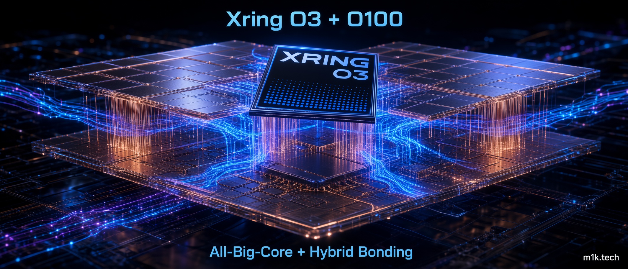
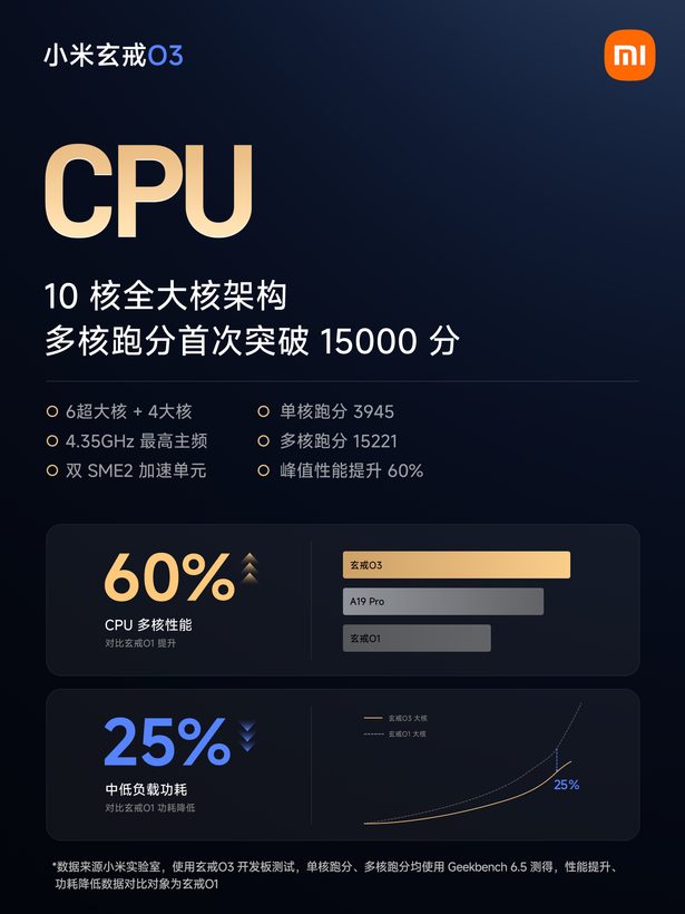
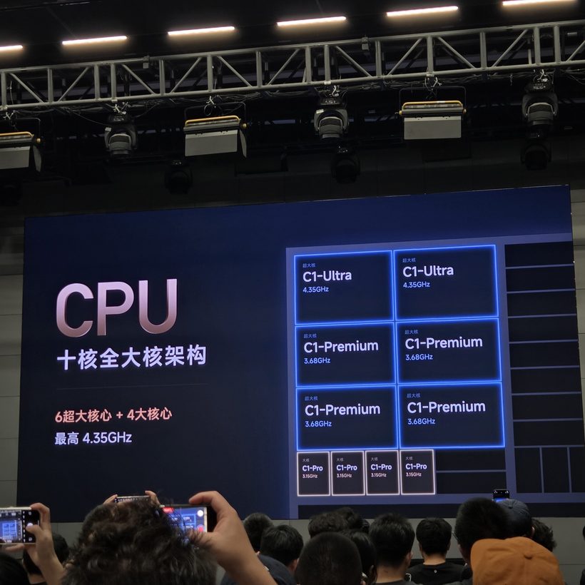
Six super-large cores and four large cores. That is the entire CPU on the Xring O3, and there is nothing underneath it. No A520-class efficiency tier, no little cluster idling at 1.8 GHz waiting to catch background work. Xiaomi built a ten-core all-big-core phone processor, then claimed daily-use power consumption dropped 25% compared with the chip that did have efficiency cores.
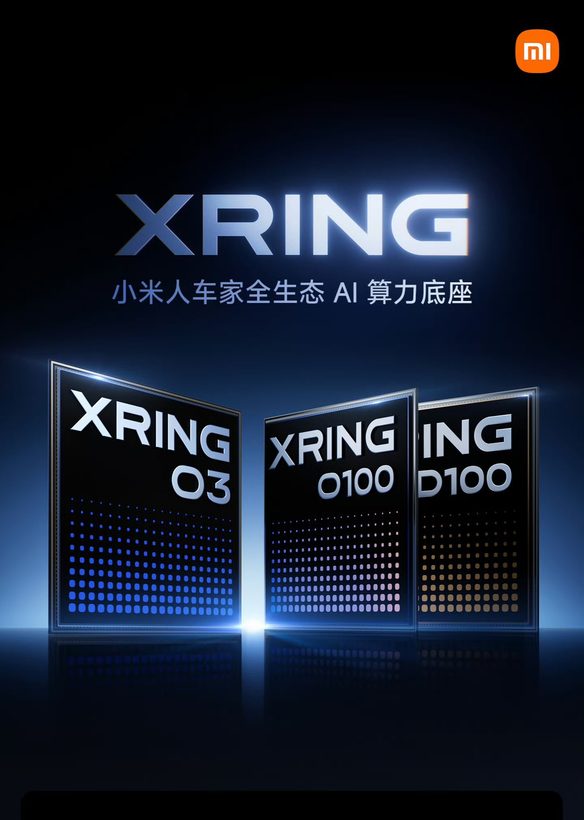
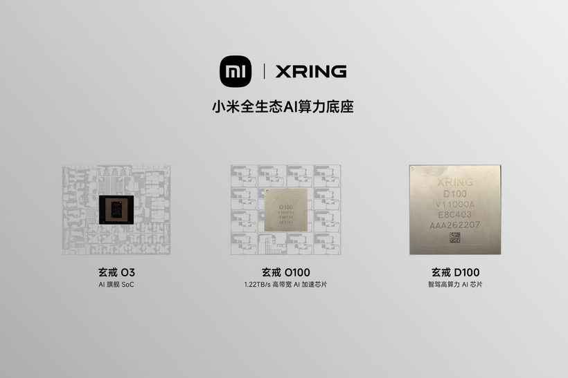
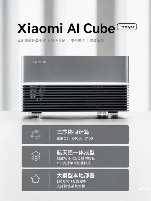
Zhu Dan, Xiaomi’s group VP, put three chips on the table in Beijing this afternoon rather than the one everyone expected: the O3 flagship SoC, an on-device AI accelerator called the O100, and a 3nm assisted-driving chip called the D100. CCTV News covered it as a national semiconductor story, which shows how they framed it. Lei Jun posted a video showing an OK hand gesture the design team etched into the O3 die, visible only under a microscope, which is the kind of thing you do when you are confident.
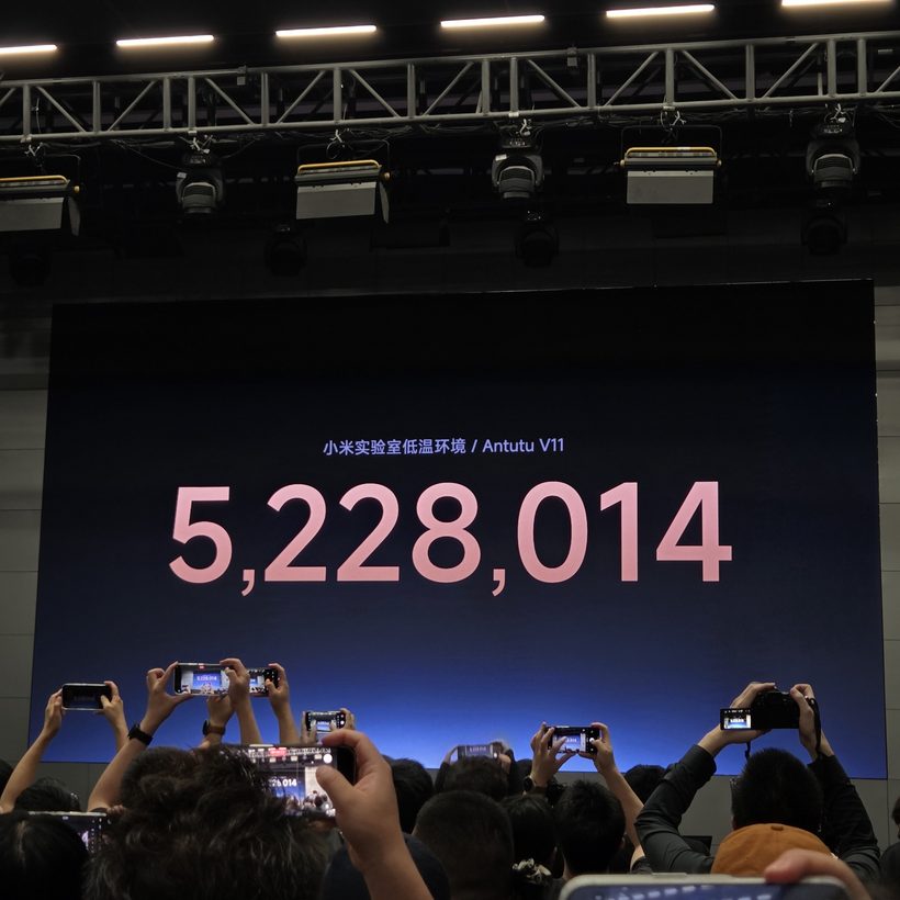
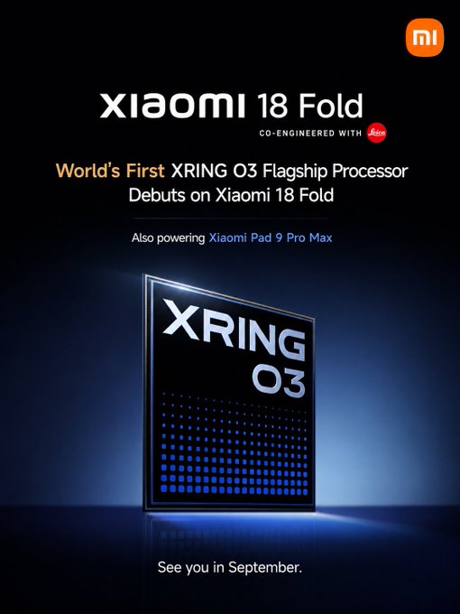
The O3 headline numbers: 3nm, 133 mm² of die, 24 billion transistors against the O1’s 19 billion, up to 4.35 GHz, Geekbench 6 multi-core of 15,221, and an AnTuTu run of 5,228,014 that makes it the first mobile platform past five million. Xiaomi says the multi-core figure clears Apple’s A19 Pro. It ships in September inside the Xiaomi 18 Fold.
What the leaks had, and what showed up
I had a draft of this post written on the leaks, and I came close to publishing it, so let me eat that publicly before anything else. The leaked frequency table that circulated from April onward described an eight-core chip in three clusters, prime at 4.05 GHz, a middle tier at 3.42, a little tier at 3.02, on roughly 20 billion transistors with the memory interface frozen at 9600 MT/s. Every one of those numbers is wrong. There is no three-cluster layout, no 3.02 GHz little core, and the memory interface is not frozen at all.
Two claims that spread through the English coverage last week are worth killing now. The first is a 68% energy-efficiency improvement attributed to Lu Weibing. That number came from an IT之家 headline reading 能效核频率飙升 68%, which means the efficiency-core clock frequency rose 68%, and 3.02 divided by 1.79 is 1.687. It was a clock speed; it got translated into a power figure, then attributed to an executive who never said it. Second, 4 GHz was a barrier no mobile chip had crossed. Qualcomm shipped 4.32 GHz in October 2024 and has been at 4.6 since last September. Even at 4.35, the O3’s prime clock sits below the Snapdragon 8 Elite Gen 5, and Xiaomi sensibly did not lead with frequency.
Why all-big-core is less insane than it sounds
Efficiency cores exist because of a specific physics problem. A wide out-of-order core burns power even when it is barely doing anything, partly through static leakage across an enormous transistor count and partly because the structures that make it fast (deep reorder buffers, aggressive prefetch, wide issue) cost energy whether or not the workload needs them. A small in-order core sipping at 1.8 GHz handles a background sync at a fraction of the energy. That has been the accepted answer since big.LITTLE landed in 2011.
The counter-argument is race-to-idle. A fast core that finishes the task in a fifth of the time and drops into a deep sleep state can beat a slow core grinding away five times longer, because leakage during that extended active window is not free either, and modern deep-sleep states are very deep. The reason nobody builds phone CPUs this way is that the argument only holds if your big cores can clock down far enough and your memory path is fast enough that they are not sitting there stalled on a cache miss, leaking, waiting for DRAM.
Which is exactly what the rest of the O3’s spec sheet is about, and it is the part I find most interesting. Xiaomi put 60 MB of on-chip cache across the main blocks, including a 16 MB system-level cache that the O1 did not have at all. Zhu Dan framed it as the SLC 补齐前代短板, filling in the previous generation’s weak spot, which is an unusually blunt admission for a launch presentation. On top of that, the O3 is the first shipping SoC to support LPDDR6, delivering 113.8 GB/s of bandwidth for a 48% increase, plus a new unified fusion bus that Xiaomi claims brings memory-access latency down to 82 ns.
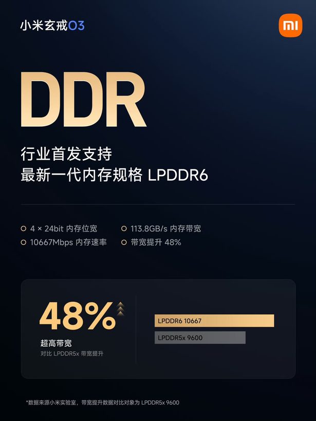
Cache and latency are what make all-big-core survivable. If your cores stall constantly, big cores are a disaster at low load. Feed them properly and the race-to-idle math starts working. I have been writing about LPDDR6 as a supply story for months, mostly through CXMT’s push to break the Korean duopoly, and it did not occur to me that the first company to actually ship it would need it as load-bearing structure for a CPU topology nobody else is attempting. Samsung was reportedly reconsidering LPDDR6 for the Galaxy S27 Ultra on cost grounds. Xiaomi took it because the architecture does not work without it.
Whether the 25% daily power reduction holds up in a real device is the question I cannot answer from a slide. Lab numbers under a controlled workload are not the same as a phone in a pocket with forty background services misbehaving, and the scheduler work required to make an all-big-core design behave under Android’s threading model is substantial. But the direction is a real architectural bet, not a spec bump, and it is the opposite bet from the one the O1 made last year with its cautious four-cluster ladder.
The GPU call I got right
A Vulkan whitelist buried in Genshin Impact‘s Android data folder surfaced two days ago, carrying two GPU entries that matched no announced product: Mali-G2-Ultra-NX in MC12 and MC16 configurations. The MC16 is now confirmed as the O3’s graphics block, and Xiaomi is the launch partner for the architecture, ahead of MediaTek.
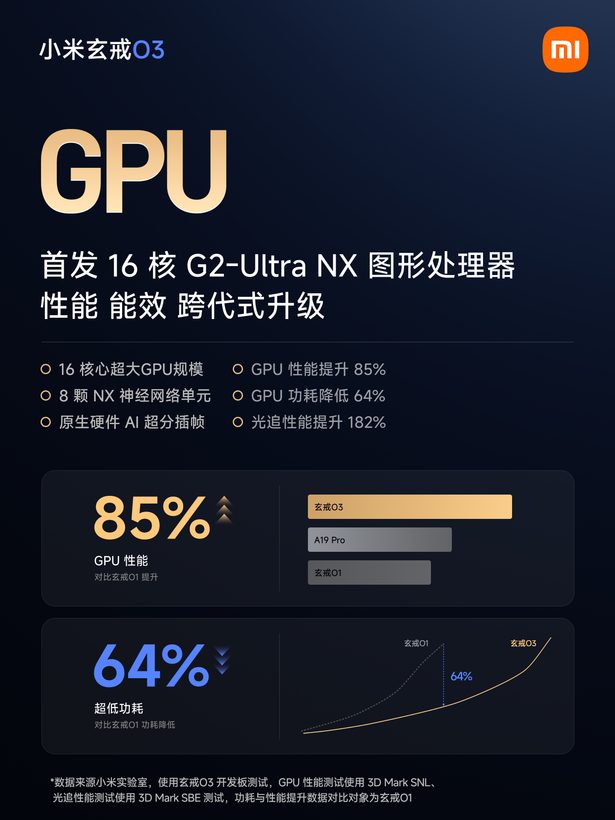
Sixteen cores again, same width as the O1’s Immortalis-G925, with 85% more raster performance, 182% more ray tracing, and up to 64% lower power at matched performance. That power figure is the one worth staring at. An 85% performance gain on the same core count and roughly the same node means the architecture did the work, and pairing it with a 64% power reduction suggests Arm’s new design is a genuine generational step rather than a clock-and-width exercise.
Hybrid bonding in a phone, while HBM backs away from it
This is the announcement that actually made me put my coffee down.
The Xring O100 is a 6nm on-device AI accelerator that pairs with the O3, built as a 3D wafer-on-wafer stack: two DRAM wafers and one NPU compute wafer bonded together with hybrid bonding. No bumps and no underfill. Direct copper-to-copper bonds, 2.58 million bond nodes at a 1.4 μm pitch. Xiaomi claims this pitch is finer than what HBM in cloud AI accelerators uses, and as far as I can tell, that claim holds. The result is 1.22 TB/s of internal bandwidth, sixteen times what a mainstream phone has, and on-device large-model inference running up to 330 tokens per second. There is a 14-core NPU dedicated to language models and a custom matrix bus Xiaomi calls XRING HB-Matrix, tying the compute tiles together. The three dies use a face-to-face metal-layer direct connection, patented, and the team spent half a year iterating the layout to stop the wafers from warping and cracking during high-temperature bonding.
Now put that next to where the memory industry actually is. Last month I wrote about Samsung and SK hynix quietly deciding to skip hybrid bonding for HBM4, pushing it out to HBM4E or HBM5, because JEDEC looked set to raise the maximum stack height and that removed the geometric forcing function. Conventional thermal compression with non-conductive film could hit twelve layers inside the looser envelope, so the two largest memory manufacturers on earth chose to defer the process risk rather than eat it. A phone company just ate it.
I want to be careful how far I push that, because the comparison isn’t clean. HBM4 ships in volume to Nvidia this year and the O100 does not ship until next year, so Xiaomi is comparing a completed design against products in mass production, which is a much easier place to be brave. Yield at volume is where hybrid bonding punishes people, and Xiaomi has not put a yield number anywhere near a slide. The wafer-warping detail is the tell: half a year of layout iteration to solve one thermomechanical problem is not a footnote; it is an admission that the process fought back hard. Ask me again when it’s in a shipping product.
Still. The reason memory bandwidth is the wall for on-device language models is that you have to stream every weight through the memory interface for each token you generate, so token rate is bounded by bandwidth almost independently of how much compute you have. Sixteen times the bandwidth is not an incremental improvement to that problem; it is a different problem. And Xiaomi got there by stacking DRAM directly onto the compute die instead of waiting for the memory vendors to solve it, which is a strategically different answer than anyone else in mobile is giving.
The 160 GB claim on the driving chip
The D100 is a 3nm assisted-driving chip with a 20-core CPU and a 16-core NPU, which Xiaomi calls China’s first 3nm smart-driving silicon. The number that jumped out is memory capacity: up to 160 GB on a single chip, enough to hold a model north of 200 billion parameters locally, with multiple chips linkable over a Xring interconnect for more. Xiaomi is explicitly pitching that at developers who want local inference without cloud API bills or data leaving the building, which is a strange thing to find inside a car chip announcement and a fairly obvious signal about where this part is heading beyond vehicles. Also not shipping until next year.
The modem, and the part I got wrong
My leak-based draft argued that the baseband was the ceiling on this whole program, on the grounds that the O1 shipped without one of Xiaomi’s own and the successor reportedly would too. The O3 integrates a baseband that Xiaomi says matches mainstream flagship integrated solutions on communication performance, with overall 5G power draw down more than 20% from the previous generation. That is a much bigger deal than any CPU number on the slide, because integrating a 5G modem is the single nastiest block in a modern SoC, dense logic married to DSPs and temperamental RF, and it is the thing HiSilicon pulled off on a sanctioned domestic 7nm line while Apple has spent years struggling to do it cleanly with TSMC’s best nodes available to it.
What Xiaomi did not say is anything about global band support or carrier certification outside China, and the debut device is a China-market foldable. So the open question is not whether the silicon works, it is whether Xiaomi has done the multi-year certification slog that turns a working modem into a phone you can sell in Europe. Until that is answered, the Qualcomm supply agreement Xiaomi renewed last year still covers the global flagships, and the Xring stays a domestic hedge that gives Xiaomi leverage in a negotiating room rather than a replacement.
I am not getting into the Xiaomi 18 Fold hardware here, the wide-format hinge and the camera stack and where it lands against the Galaxy Z Fold 8 Wide. That deserves its own post once we have seen the thing.
What stays with me is the shape of the announcement, not any single number. Fifteen months ago Xiaomi shipped a competent, cautious first flagship SoC with a licensed modem and a hedged four-cluster CPU, and a lot of people, including me, read it as a credible proof of concept that would take another two generations to become a real platform. The company came back with an all-big-core CPU nobody else in mobile is attempting, the industry’s first LPDDR6 controller, wafer-on-wafer hybrid bonding that the memory giants just deferred, and its own baseband. That is not iteration. Whether the 25% power claim and the 330 tokens per second survive a real device in September is the only thing I actually care about now, and September is close enough that we will not have to argue about it for long.
Sources
- DoNews via TGBUS, 小米发布三款玄戒自研芯片,覆盖 AI 手机、高带宽计算与智驾领域, 24 August 2026
- IT之家, 小米玄戒三芯齐发,央视新闻报道称“中国芯片产业再突破”, 24 August 2026
- Sina Finance, 雷军曝光小米玄戒 O3 隐藏彩蛋, 24 August 2026
- NetEase Tech, 小米公布玄戒 O3 芯片架构, 24 August 2026
- Notebookcheck, Upcoming Dimensity 9600 Pro and XRing O3 GPUs may have leaked from Genshin Impact, 22 August 2026
- IT之家, 小米自研芯片玄戒 O3 曝光:主频突破 4GHz、能效核频率飙升 68%, 29 April 2026
- GSMArena, Xiaomi 15S Pro debuts with in-house Xring O1 chipset, 22 May 2025