Three weeks after a magnitude 7.1 earthquake rattled the same prefecture hard enough to hit max intensity on Japan’s seismic scale, Sony and TSMC signed a legally binding, 747 billion yen agreement to build their next image sensor plant right there. Not somewhere safer. Same postal code as the damage.
That’s the detail that stuck with me more than the headline number. Advanced Vision Semiconductor Manufacturing Corp, the joint venture the two companies signed into existence on August 11, will sit in Koshi City, just north of Kumamoto city, a few minutes from where TSMC already runs its JASM logic fab. Sony is putting in 465 billion yen (about $2.9 billion), mostly by handing over a brand-new fab it already built in Koshi, plus cash. TSMC is writing a 282 billion yen check, roughly $1.8 billion, straight cash. Sony keeps 68% and full operational control as a consolidated subsidiary; TSMC gets the rest and a seat at the table, but Sony appoints the Representative Director. Far from a merger of equals, this is Sony buying TSMC’s process technology at scale while staying firmly in the driver’s seat.
None of this came out of nowhere. The two companies announced a preliminary agreement back on May 8, months before the quake, so what happened this week is really the moment the paperwork caught up to a decision that was already made. That timing matters for how I read the earthquake risk here: I don’t think this venture survived the quake through confidence, I think it survived because backing out of a half-billion-dollar handshake three months in is its own kind of disaster, arguably worse than the one already on the ground. I wrote a few days back about JASM’s Kumamoto fab posting its first real profit right as the quake complicated the sequel plant. This JV is the sequel plant.
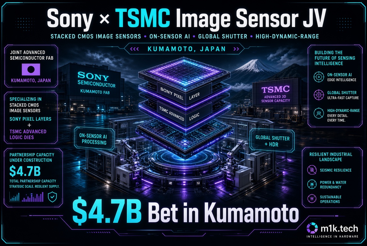
What’s actually being built is worth slowing down on, because “next-generation image sensors” undersells it. TSMC has fabricated the logic dies for Sony’s stacked CMOS sensors for years already, the layer that handles readout, on-chip processing, and increasingly on-sensor AI inference sitting beneath the photodiode layer everyone actually associates with “camera sensor.” What this JV does is take that existing foundry relationship and turn it into dedicated capacity Sony doesn’t have to fight Apple and Nvidia for. TSMC’s advanced nodes are the tightest bottleneck in the industry right now, I’ve written about the CoWoS allocation fights more than once, and a phone sensor logic die competing for wafer starts against an H200 or an A19 Pro is a fight the sensor loses every time on priority. A co-owned fab changes that math entirely. Sony brings the pixel architecture, the color science, the decades of dominance in the actual photography side; TSMC brings a logic process node advanced enough to stack a real memory layer under the pixels for genuine global shutter and better HDR pipelines without murdering die size. That’s the technical trade being made here, and it’s a smart one on paper.
The market context makes the urgency clearer. Sony already controls more than half of the global image sensor market by value, which sounds unassailable until you remember Samsung’s LSI division has been closing the gap on flagship phone sensors for three straight generations, and the Chinese CIS makers, OmniVision, GalaxyCore, and the rest, have gotten uncomfortably good at the mid-tier where the actual unit volume lives. A dedicated logic supply chain that nobody else can touch is a moat, not a nice-to-have. I’d also flag the AI angle both companies leaned on in the press language, sensors for robots and machines, because that’s clearly the second act here even though the JV’s stated first job is smartphone sensors. Machine vision at scale wants exactly the kind of stacked, low-latency, on-sensor processing this partnership is built to produce.
Where I get less comfortable is the funding structure. Buried in the announcement is a line about the JV “considering a separate funding scheme” to hit its target capacity, contingent on government support that hasn’t been confirmed yet. That’s not a small footnote. It means the 747 billion yen on the table today may not be the number that actually gets this thing to volume production, and Japan’s government has been generous with chip subsidies but not infinitely so. Watch that line as closely as you watch the earthquake recovery.
Volume production is targeted for 2029, with one report putting 300mm wafer output specifically at May of that year, which gives Kumamoto roughly three and a half years to fully rebuild its chip-region infrastructure, water and power included, while simultaneously standing up an entirely new fab on top of the existing shell Sony already built. I’m not going to pretend I know how fast that recovery happens. Nobody does yet, not even the companies signing the check. What I’ll say is that TSMC extending outside pure logic into a co-owned sensor fab is a new move for them in Japan, and it’s happening in the one region where the ground already proved it can’t be fully trusted. Sony and TSMC are betting $4.7 billion that Kumamoto rebuilds on schedule. I hope they’re right, because if the region can’t hold up its end, this becomes a very expensive lesson in geographic concentration risk that the whole industry already should have learned from Fukushima.