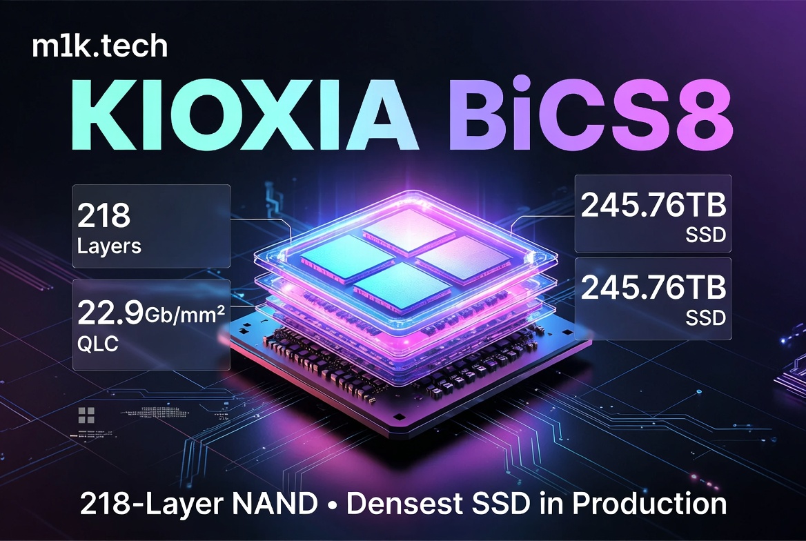
SK hynix is shipping 321 layers. Samsung sits at 286, Micron at 276, and even YMTC out of Wuhan just showed a 294-layer part at Computex. KIOXIA’s newest flagship flash, the eighth-generation BiCS FLASH the company has stuffed into every blog post for the past year, tops out at 218. On the one number the entire industry uses to keep score, KIOXIA is dead last among the majors, and it isn’t close.
Then you look at what’s actually shipping. The single highest-capacity SSD you can buy in mid-2026, the 245.76TB LC9, runs on that “losing” flash. That gap between the scoreboard number and the product is the whole story, and it’s the part KIOXIA’s own marketing keeps fumbling.
Layer count measures one thing: how many times you’ve stacked a memory cell vertically. More floors in the same footprint, more apartments per square millimeter. It’s the headline because it’s easy to print on a slide and it correlates with density. It is not the only lever. You can shrink the cells laterally, run more planes in parallel, and stop wasting silicon on dummy structures that don’t store anything. KIOXIA picked that lane instead of the layer-count drag race, and the engineering that makes it work has two names.
CBA, CMOS directly Bonded to Array, builds the control logic and the memory array on two separate wafers and bonds them together at the end. Older BiCS generations stacked the cells on top of the CMOS on a single wafer and then had to pick a thermal budget that wouldn’t cook either one. Splitting the wafers means the cell array can take a high-temperature anneal that improves reliability without frying the logic underneath, because there’s no logic underneath yet. The second trick, OPS (On Pitch SGD), rips out the dummy memory strings that used to sit under the insulator slits and packs the live strings tighter. Dull on its own. Together they land KIOXIA at 18.3 gigabits per square millimeter on the 1Tb TLC die, which the company says is the densest anything in the 2xx-layer class, hit with roughly 5% fewer layers than the ~230-layer competition.
The QLC version is where it gets a little ridiculous. When TechInsights tore down the 2Tb QLC die, it measured 22.9 Gb/mm², above SK hynix’s G9 TLC and comfortably past Micron’s 276-layer part at around 21. The company with the fewest floors built the most crowded floors in the building. This is the metric that decides cost per bit, and it’s the one nobody prints on a keynote slide because “218” looks small next to “321.”
Here’s roughly where everyone sits on flash that’s actually in production right now:
| Maker | Top layers in production | Next-gen approach |
|---|---|---|
| SK hynix | 321 (V9) | V10, ~300+, wafer bonding, ~2027 |
| YMTC | 294 (Xtacking 4.0) | hybrid bonding, already on it |
| Samsung | 286 (V9) | V10, 400+, hybrid-bonded CoP |
| Micron | 276 (G9) | undisclosed |
| KIOXIA / SanDisk | 218 (BiCS8) | BiCS10 at 332, in development |
The payoff ships as the LC9. Stack 32 of those 2Tb QLC dies into a single 154-ball BGA package measuring 11.5 by 13.5 millimeters, smaller than a postage stamp, and you’ve got 8TB in one chip. That’s an industry first on its own. Wire about 30 of those packages to a controller and you hit 245.76TB in an E3.L drive. It took Best of Show at Flash Memory Summit last August and KIOXIA was back waving it around at CES in January. For scale: one of these replaces eight 30TB hard drives, and it does random reads something like 1,800 times faster than the spinning rust it’s displacing. I find that genuinely hard to picture, a quarter of a petabyte in a 2.5-inch shell.
Now the part KIOXIA would rather you skim. This is QLC, four bits per cell, and it acts like it. The LC9 reads at up to 12 GB/s but writes at 3, which is slow for a PCIe Gen5 drive, and endurance is rated at 0.3 drive writes per day. You are not putting a database write log anywhere near this. It’s read-mostly bulk storage: AI training corpora, vector databases, the media archives you write once and read forever. That’s a real and fast-growing market, and the drive is built for it on purpose. But the KIOXIA blog post that kicked this off pitches “ultra-fast” performance and an “industry-leading NAND IO speed of 3.6 gigabits per second,” and that number is quietly lying. BiCS8’s interface runs at 3.2 Gb/s. The 3.6 figure belongs to the ninth-generation flash KIOXIA started sampling last summer, not the gen 8 the post is supposedly about.
The power line has the same tell. The post brags about “up to 179% improvement in power efficiency,” and four footnotes down it cops to measuring that against BiCS generation 5, the 112-layer flash from around 2021. Comparing your 2025 silicon to a 2021 part and headlining the delta isn’t false, it’s just not the comparison anyone reading the big number assumes they’re getting. When a tech brief makes you chase a footnote to find out which generation it’s beating, the footnote is usually the actual news.
So is this a good announcement or a bad one. Depends which KIOXIA you mean. The engineering bet is smart and it’s the contrarian kind I like: fewer layers means fewer of the brutal high-aspect-ratio etch steps that murder yield, which means lower cost per bit, which is the only line item a hyperscaler buying flash by the petabyte actually reads. KIOXIA traded the bragging number for the spreadsheet number and shipped a real, record-setting product out the other side. I respect the discipline of that.
The strategy is where I cool off. CBA is wafer-to-wafer bonding, and wafer bonding is exactly what SK hynix and Samsung are both pivoting to for their next generation. SK hynix’s V10 splits the cell stack and the peripheral onto separate wafers and bonds them, with a test line this year and production targeted for 2027. Samsung’s 400-plus-layer V10 leans on hybrid-bonded cell-on-peripheral. The architectural trick KIOXIA is a generation ahead on is the one its rivals are about to adopt at 300-plus layers, and when they do, the density edge that justifies the low layer count could thin out fast. KIOXIA’s own ninth-gen flash doesn’t fix this, by the way: it’s a cost-optimized rebuild on a 120-layer base, not a layer jump. The real catch-up is BiCS10 at 332 layers, and that’s still in the lab.
I’m leaving the SanDisk angle alone here, the fact that these fabs are a KIOXIA–SanDisk operation now that Western Digital spun the flash business out, because that changes who books the revenue and it’s its own post. On the silicon: the LC9 is the best high-capacity QLC drive you can buy today, and 218 layers was the right call for this round. Whether “most bits per layer” survives contact with rivals who are about to bond wafers too, at more layers, is the open question. KIOXIA spent its architectural lead on a record drive instead of banking layers. Smart for 2026. Ask me again when Samsung’s 400-layer hybrid-bonded QLC actually ships.