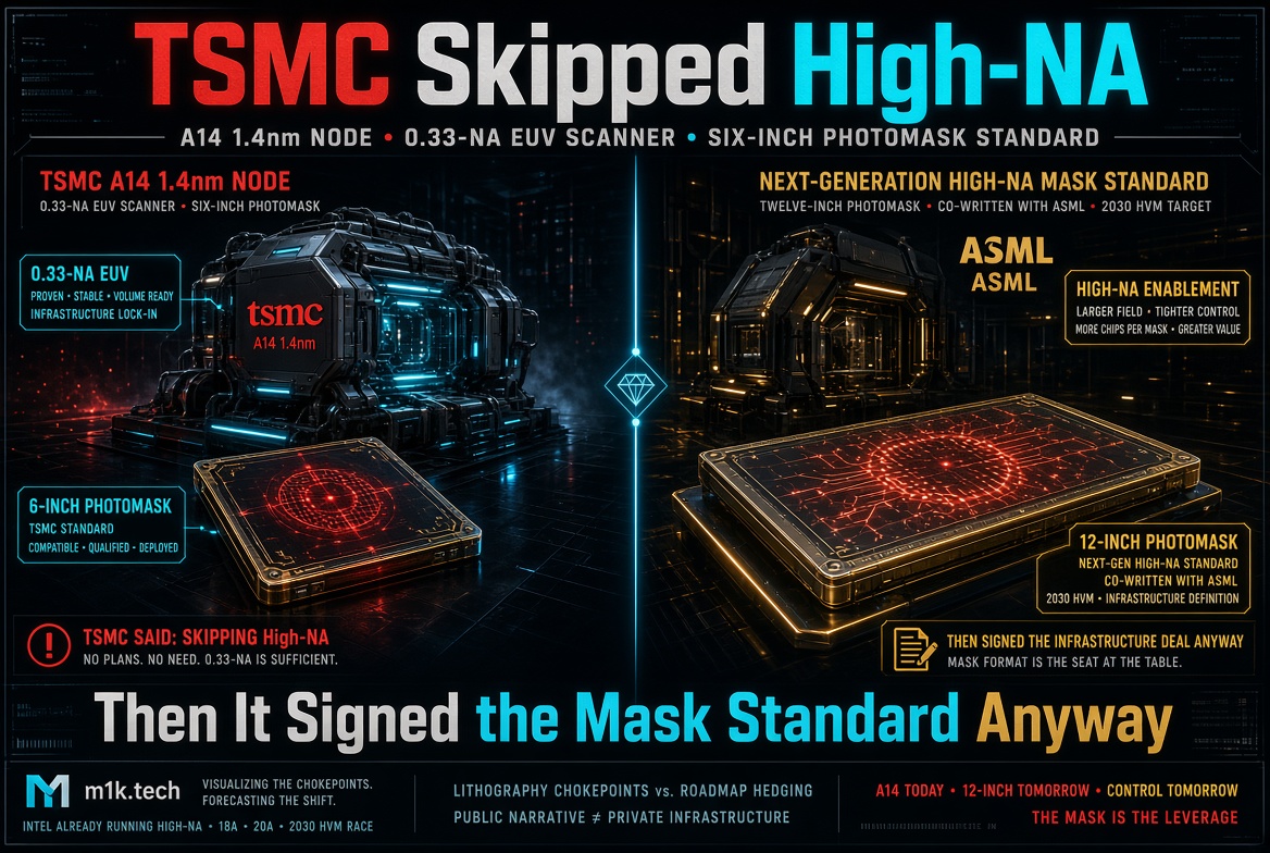
Three weeks ago I wrote about TSMC SVP Kevin Zhang telling a room full of engineers that the company’s 1.4nm A14 node would skip ASML’s High-NA EUV tool entirely, standard 0.33 numerical aperture lithography and multi-patterning tricks instead of the $380 million machine, because minimizing mask count mattered more than the resolution jump. On Tuesday, TSMC signed a joint initiative with ASML to build the next-generation High-NA infrastructure anyway.
The announcement itself is about photomasks, not chips, which is why it’s easy to skim past. High-NA EUV currently runs on the same six-inch masks standard EUV has used for years, and ASML and TSMC now want to move the whole industry to twelve-inch masks instead, a format that’s supposed to boost scanner productivity and cut chipmaking costs by removing a stitching constraint that shows up once transistor patterns get complex enough. The two companies are targeting a twelve-inch mask pilot line by 2031 and full readiness for advanced node production by 2033. Buried in the same release is the part that actually matters: TSMC now says it will bring High-NA into high-volume manufacturing for advanced nodes starting in 2030.
That’s not technically a contradiction of what Zhang said in August, and I want to be fair about that before I get to why it still bugs me. A14 hits mass production around mid-2028. A 2030 High-NA commitment lines up with whatever comes after A14, not A14 itself. Zhang’s actual claim was narrower than the headlines it generated; mine was that TSMC would still need the tool, just not for this specific node yet. Skip doesn’t mean opt out, and TSMC just spent a press release proving it.
Samsung joined the same initiative, and its own timeline is a mess I can’t fully untangle. Samsung says it will use ASML’s High-NA machines to produce DRAM starting in 2028 in one part of its own announcement, then says it’s adopting the technology in 2030 in another, and I’ve seen both years reported straight-faced by outlets covering the same release. I’m not going to pretend I know which one is the typo. What I do know is that Samsung’s actual production node for 1.4nm sits at 2029, a full year behind TSMC, so either date puts High-NA DRAM ahead of Samsung’s own logic roadmap, which is its own small oddity.
Intel is the one company in this story that isn’t hedging anything. It bet on High-NA from the start for select layers of its own 14A node, and at the same SPIE conference where ASML and TSMC made their photomask announcement, Intel disclosed that its High-NA tools have now processed over a million wafers combined across certification, R&D, and actual Panther Lake production, more than every other chipmaker’s High-NA output put together, going by ASML’s own estimate of roughly 500,000 wafers industry-wide as of April. Intel is the only company here running the expensive machine at real volume instead of talking about the year it might start.
I don’t think Tuesday’s announcement means High-NA suddenly became load-bearing for TSMC’s roadmap. A14’s own numbers, 15% better performance or up to 30% lower power over 2nm plus a 20 to 23% density gain, are TSMC’s proof that standard EUV plus clever masking still works fine for now. What changed isn’t the physics; it’s who gets to help write the twelve-inch mask standard the entire industry will eventually run on. ASML holds the only chokepoint that matters here, and Intel already had a seat at that table by virtue of using the tool in production. Sitting out the 12-inch initiative while Intel and whoever else signs on decide the format everyone eventually inherits is a worse position than committing to a 2030 date you might slip later. TSMC didn’t change its mind about the tool. It changed its mind about who gets to design its replacement.
I was skeptical of the skeptics back in August, and I still think High-NA arrives on everyone’s roadmap eventually, the same way every proposed alternative to ASML’s monopoly keeps turning out to be years away from mattering. I didn’t expect TSMC to prove my instinct right three weeks after making the opposite case in public. Zhang wasn’t wrong about A14. He just wasn’t describing the whole roadmap, and I should have caught that the first time.
Sources
- ASML and TSMC joint press release, ASML and TSMC Announce Initiative to Pioneer Industry Transition to Large-Format Photomasks for High NA EUV, September 8, 2026
- CNBC, Samsung and TSMC commit to ASML’s High NA EUV machines as AI chip demand grows, September 8, 2026
- BigGo Finance, Intel Foundry passes 1 million wafers processed on High-NA EUV, September 8, 2026