TSMC’s 3nm line is on pace to hit 180,000 wafer starts a month by early Q4, two to three months ahead of schedule, and its 1.4nm A14 fab in Taichung is running ahead of its own timeline too. That’s the headline pairing making the rounds this week, and the wafer-start number is the less interesting half of it.
The acceleration itself is straightforward once you follow the money. Nvidia, AMD, and Broadcom have been booking 3nm capacity faster than even TSMC’s own optimistic projections, and the company has been converting existing 5nm lines to pick up the slack rather than waiting on new buildings. Both nodes share the same FinFET architecture and lean on the same ASML EUV tools, so a retooled 5nm line can fold into 3nm production in six to twelve months instead of the years a new fab takes. It’s the same crunch that turned the Kumamoto fab profitable the same week an earthquake complicated its own expansion plans, and the same crunch behind the price hikes TSMC pushed through this year with another round penciled in for 2027. Demand hasn’t cooled once in eighteen months. It’s just outrun every schedule TSMC has published against it.
2nm is ramping on the same trajectory, and that interests me more than the headline 3nm figure. Monthly starts on the gate-all-around node that finally moved TSMC off FinFET are tracking toward 80,000 by early Q4 and close to 100,000 by year end, up from roughly 50,000 to 60,000 through the first half of the year. Combined 2nm and 3nm output crossing 260,000 wafers a month by Q4, with a path to 400,000 by 2028, is the real supply story. It’s the clearest evidence yet that TSMC has stopped managing scarcity and started actively expanding the ceiling on how much AI silicon the industry can physically produce.
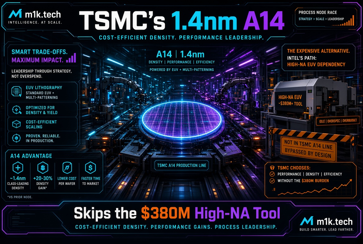
The bigger surprise is in Taichung. Construction on TSMC’s 1.4nm A14 fab in Taichung, a $49 billion project that broke ground in November, is also running ahead of schedule. The first of four planned buildings should be done before April 2027, pilot production could start as early as Q3 2027, and mass production is now targeted for mid-2028, earlier than the company had previously indicated. Buried in that timeline is a decision TSMC SVP Kevin Zhang made almost in passing at the company’s North America Technology Symposium: A14 isn’t going to use ASML’s High-NA EUV tools at all.
That’s a real choice, not a footnote. Standard EUV, the kind TSMC runs today, has a 0.33 numerical aperture and resolves patterns down to about 13nm. High-NA pushes that to 0.55 and 8nm resolution, and it costs roughly $380 million a unit, two to three times a standard EUV tool, with a single exposure running up to 2.5 times more than the equivalent standard pass. Zhang’s framing was blunt: TSMC can hold A14’s process complexity steady through multi-patterning tricks without paying that premium, and minimizing mask-count growth generation over generation is, in his words, “very important to provide a cost-efficient solution.” Intel made the opposite bet. 14A, Intel’s own 1.4nm-class node, uses High-NA for selected critical layers, and after watching how much 18A-P still has to prove on its own, I’m not convinced Intel can afford to be wrong about what that tool buys it.
I’m skeptical of High-NA skeptics as a rule, mostly because ASML’s own roadmap treats the tool as inevitable past a certain node. But TSMC skipping it for A14 while still claiming 15% better performance or up to 30% lower power over 2nm, plus a 20 to 23% density gain, is a strong argument that the tool isn’t load-bearing yet. Samsung isn’t even in this conversation for what it’s worth: its own 1.4nm target sits at 2029, a full year behind TSMC and further behind Intel.
What matters here is simpler: TSMC just told the industry it doesn’t need the single most expensive lithography tool that exists to stay two years ahead, and Intel is the one that has to hope it was wrong to think it did.
Sources
- Tech Times, “TSMC Accelerates 3nm Output Months Early; 1.4nm Factory Beats Schedule”, August 8, 2026
- TrendForce, “TSMC’s 3nm Monthly Wafer Starts to Hit 180K by Early 4Q26”, August 3, 2026
- TrendForce, “TSMC’s 1.4nm Fab Ahead of Schedule”, July 30, 2026
- Electronics Weekly, “TSMC ahead of schedule with 1.4nm fab”, August 2026
- Bits&Chips, “TSMC skips High-NA for A14”
- Tom’s Hardware, “Intel Commits to 14A Mass Production in 2028”