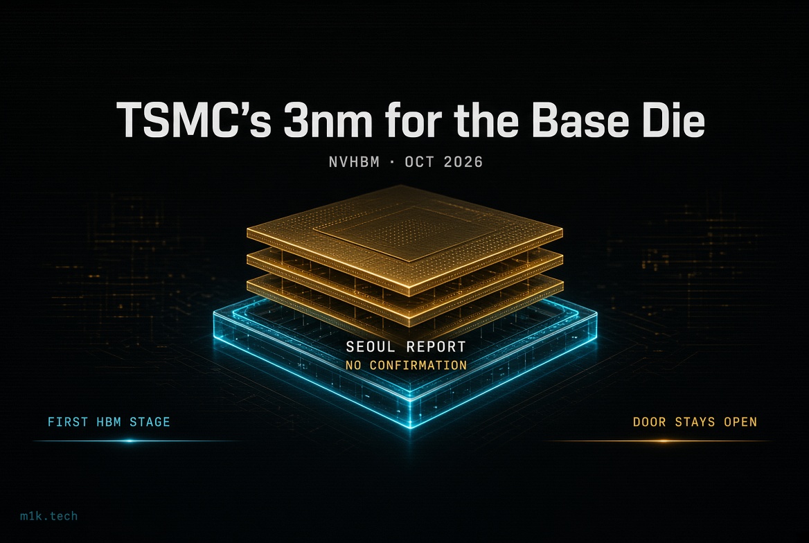
In August, Samsung said its 2nm Exynos could beat Qualcomm’s next flagship. For the bottom layer of Nvidia’s next memory stack, it will reportedly use TSMC’s 3nm process instead. Seoul Economic Daily published the claim on Sunday and Reuters relayed it; I found no confirmation from Samsung, Nvidia or TSMC, and everything below carries that caveat.
The base die is the logic chip at the foot of an HBM stack, and it largely decides how fast data moves in and out. Nvidia’s NVHBM, unveiled in August, pulls the company’s own memory controller into that die, a job the GPU used to do. According to the newspaper, Nvidia asked Samsung, SK Hynix and Micron to build those base dies on TSMC’s 3nm and to use sixth-generation DRAM for the core dies above them. Samsung agreed after an internal review.
It would be the first time Samsung works with TSMC at the HBM manufacturing stage.
I can’t verify any of the performance claims that travel with the story: a physical layer shrunk 60% against standard HBM, up to 30% more bandwidth and 15% less power than standard HBM4E. A separate claim from unnamed industry sources puts TSMC’s yield on the process above 90%, versus roughly 60% for Samsung’s comparable 2nm. Those are two different nodes, so I read the number as an argument for the decision rather than a benchmark, though if it is anywhere near right it explains why Nvidia wouldn’t wait around to find out. My piece on Samsung’s 2nm Exynos claim was about a process that had caught up. This is the other side of that coin.
What Samsung keeps matters as much. The report says it holds on to its in-house model for standard HBM and for custom parts sold to other customers, and that it is weighing whether its own foundry could make NVHBM base dies if demand outruns TSMC’s capacity. So the door back stays open, on paper.
This is the half I care about. In July I called the $200 billion Broadcom deal a foundry stress test, and here is a smaller, stranger one: the biggest buyer of HBM telling a memory maker that the logic at the bottom of the stack gets built by the rival it fights at the leading edge. Samsung’s selling point has been memory, foundry, and packaging under one roof, and for this product, the roof has a TSMC-shaped hole. If you want the groundwork on where the stack is heading, the HBM4 piece is the place to start.
Samsung and SK hynix shares fell 9.5% and 11.1% on 15 October on AI doubts, which I covered in the Kospi sell-off post. This report doesn’t touch that question, but a memory maker handing its most valuable layer to a foundry competitor won’t help the story investors are telling themselves.
Nothing is confirmed. If Samsung’s own fab ends up making any of these base dies, I’m wrong about the hole in the roof, and I wouldn’t bet on that happening this year.
Sources
- Reuters: Samsung to use TSMC technology for Nvidia’s next-generation memory chips, Seoul newspaper says, 18 October 2026
- Verdict via Yahoo Finance: Samsung collaborates with TSMC for Nvidia’s custom HBM chips, 19 October 2026
- SamMobile: Samsung agrees to let TSMC make custom Nvidia NVHBM base die, 19 October 2026