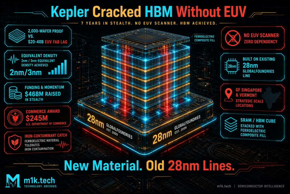
Kepler Computing spent seven years in stealth betting that the memory industry’s answer to scarcity, building more EUV-dependent fabs, was solving the wrong problem. This week its cofounder and CEO, Debo Olaosebikan, said so out loud for the first time.
Kepler claims it doesn’t need extreme ultraviolet lithography at all to hit 2nm or 3nm-equivalent density on SRAM, and that a similar 3D stacking approach can push density on HBM, the stacked memory that’s become the single most fought-over component in AI hardware. Both claims run through a proprietary composite material built around ferroelectrics that cofounder and CTO Sasi Manipatruni says took 35 material iterations to land on. The manufacturing itself runs on GlobalFoundries’ existing 28-nanometer lines in Singapore and Vermont, not a fab built from scratch for the purpose.
That last detail is the entire pitch. A new HBM fab costs $20 billion to $40 billion and takes years to come online, which is exactly the kind of lag that let China’s own DRAM insurgent CXMT close so much ground so fast on the low end, and the same lag that had Samsung passing a flat $100 memory surcharge onto every foldable this summer despite manufacturing the memory itself. Kepler’s argument is that you don’t need a new category of fab at all, just a new material system dropped into equipment that already exists.
The money backing that argument is real: $468 million raised from GlobalFoundries, Intel Capital, AMD Ventures, the UK fund Baillie Gifford, and Bill Gates through his Gates Frontier fund, plus a Commerce Department commitment of up to $245 million announced in July for exactly this kind of 3D ferroelectric memory work. GlobalFoundries senior vice president Ed Kaste calls the approach the sweet spot of the foundry’s strategy precisely because it skips new lithography tools, though he’s candid about the catch too: the composite includes iron, which he says is “a tough contaminant to introduce into a production facility,” meaning Kepler needs either dedicated equipment or full encapsulation to keep it from spreading through the fab.
The skepticism writes itself once you get past the pitch. Kepler has run its process on roughly 2,000 wafers total. First HBM samples are targeted for later this year, the Singapore line ramps next year, and US production doesn’t start until 2028, the same year Apple is already testing DRAM from CXMT just to keep its own China-market supply diversified. Austin Lyons, a chip analyst at Creative Strategies who wasn’t briefed on the announcement, put the real question plainly: whether the contamination and tooling problems can be solved at a scale that’s actually worth the cost, not whether the physics works in a lab.
Two thousand wafers prove the chemistry works. It doesn’t prove Kepler can hit the yields SK Hynix and Micron need to start worrying about by 2028, and I’ve watched enough EUV-adjacent moonshots (Substrate’s nanoparticle lithography pitch got the same skeptical reception late last year) to want more than a glossy stealth-exit profile before I call this the fix. I do think Kepler picked the right year to make the argument. The industry just spent an entire summer proving it doesn’t have another one to spare.
Sources
- WIRED, A Stealth Startup Thinks It Just Hacked the Memory Shortage, September 9, 2026
- ExecutiveGov, Commerce Department Announces CHIPS R&D Incentives, July 30, 2026
- Reuters, China’s AI chipmakers raise prices as high-bandwidth memory shortage bites, September 10, 2026