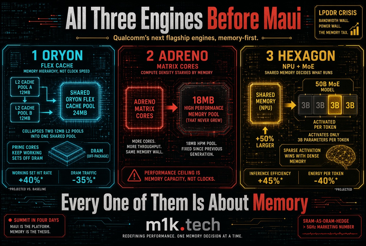
Qualcomm has now put all three engines of its next flagship on the record, one post at a time, and the pattern only shows up if you read them together. The Oryon CPU landed on 25 August, Adreno on 2 September, Hexagon on 10 September. Three different authors, three different subsystems, three different audiences. Each one leads with a claim about keeping data off the memory bus.
That is not how chip marketing usually works. The CPU post is supposed to sell you gigahertz, the GPU post is supposed to sell you frames, and the NPU post is supposed to sell you TOPS. Instead, the CPU post says memory constraints across industry and pitches a cache reorganization as the fix. The GPU post spends its best paragraphs on an on-chip pool that keeps tiles and frame buffers from touching DRAM. The NPU post’s second bullet is a 50 percent larger shared memory, and its headline model architecture is chosen specifically because it activates a tenth of its parameters per token.
I have written the GPU piece and the NPU piece separately, and I am keeping them separate because each deserves its own argument. This one is the platform read: what the three say jointly, how it compares to what Qualcomm shipped last year, what the competition did while Qualcomm was teasing, why the business case looks the way it does, who is actually getting these chips, and what the whole thing is in service of. The Summit opens in Maui on the 22nd, which gives this four days of shelf life.
Where 5GHz actually comes from

Oryon got to 5GHz almost a year ago. The X2 Elite Extreme boosted two of its twelve prime cores to 5.0GHz, and Qualcomm called it the first Arm CPU to get there, so the word carrying the weight in the new claim is mobile. That is not a dodge. The laptop part hit that clock with 53MB of cache and the thermal headroom to draw real power, and landing the same frequency in a passively cooled slab running off a battery is a different problem in every respect that matters.
Qualcomm’s framing is unusually specific about where the clock came from: not a process node alone. They designed the microarchitecture, the implementation choices behind it, and the CPU subsystem around it, then tuned the three together. Read that as a shot at everyone shipping licensed cores on a new node and calling the frequency their own achievement.
The detail that didn’t make the blog post but did make Qualcomm’s spec card is more interesting than the number: each prime core sits on its own clock domain and can ramp independently, instead of the cluster moving in lockstep. That is a real power-management change, and it pays off in exactly the workload Qualcomm keeps describing, where one core does orchestration work while the others idle or run something unrelated. A single 5GHz core that can boost alone, without dragging its neighbor up with it, costs a lot less battery than a cluster that boosts together.
Buried under the frequency line is a second claim worth flagging. Qualcomm says the clock is not doing all the work and that IPC carries part of the gain. That is the honest metric, and it is also the one they have declined to quantify: no percentage, no baseline against the Gen 5 core. Oryon has claimed per-clock improvements at every generation, so until somebody runs real code on real silicon, this is a promise rather than a number. A Geekbench 7 listing that surfaced on 10 September put a prime core at 5.11GHz, which suggests 5.0 is a rated floor for the higher tier rather than a ceiling, but a single unverified database entry is not a benchmark, and I am not treating it as one.
Some history for scale. The first mobile Oryon, in the Snapdragon 8 Elite, ran its prime cores at 4.32GHz in October 2024. Last September’s third-generation Oryon in the 8 Elite Gen 5 pushed to 4.6GHz on TSMC’s N3P, paired with six performance cores at 3.62GHz. So this is roughly a 9 percent clock jump on top of a full node transition, and the node is where a lot of the headroom comes from, whether or not Qualcomm wants to say so. TSMC quotes N2 at 10 to 15 percent more speed at the same power against N3E, or 25 to 30 percent lower power at the same speed, and N2P raises that to roughly 18 and 36. You spend that budget once. Qualcomm appears to have spent a lot of it on frequency.
The die is reportedly around 134 mm² for the top part, up from 126.2 mm² on the Gen 5, which is the wrong direction on a denser node unless you are adding a meaningful amount of silicon. Cache is silicon.
The two twelve-megabyte pools that used to sit apart
Here is what Flex Cache is actually fixing, and it is a problem Oryon has carried since it was a laptop core.
On the Snapdragon 8 Elite Gen 5, the CPU’s L2 is not one cache. It is two: a 12MB pool for the two Prime cores, and a separate 12MB pool for the six Performance cores. Twenty-four megabytes on the spec sheet, but no single core can ever see more than twelve of it. Underneath that sits an 8MB system-level cache shared with the ISP, the NPU, and everything else on the die, which is why calling it an L3 has always been misleading. The GPU has its own High Performance Memory and does not share it.
That split has a cost, and it was baked in from the beginning. Oryon has always been quad-core clusters sharing a fat L2, a structure Gerard Williams brought over from the Apple cores he designed before it. On the PC side, that showed up in measurement: core-to-core transfers inside a cluster were fine; cross-cluster transfers were expensive, unusually so for a monolithic chip at consumer core counts. Every time Android’s scheduler moves a thread from a Prime core to a Performance core, that thread’s working set is in the wrong pool. It starts cold. The data either gets pulled across the interconnect or refetched from DRAM, and the second option hurts.
Flex Cache collapses that. One pool, allocated dynamically by workload, reachable by cores of different types. Qualcomm’s specific claim is that Prime cores can draw on the entire pool when a workload demands it, so a large working set stays resident instead of spilling once it outgrows its cluster’s share. The leaked figure for the standard part is 16MB of L2 shared across all cores plus 6MB of system-level cache, with the higher tier getting 8MB of SLC.
Do the arithmetic and something uncomfortable falls out. Gen 5 has 24MB of L2 in total, and the leak says Gen 6 has 16. If those numbers are right, Qualcomm shrank total CPU cache by a third and made what remains fully shared. For scale, the laptop Oryon carries 53MB across the die. Stranding a chunk of that behind a cluster boundary is an affordable waste; doing the same thing with 16MB is not, which is the honest reason the pool has to be flexible rather than split. For a single-threaded burst on a Prime core, that is a clear win: twelve megabytes visible becoming sixteen. For a heavily threaded workload spread across all eight cores, sixteen shared is less than twenty-four split, and now the Prime cores and the little ones compete for the same lines.
Whether that trade lands depends entirely on the allocation policy, and Qualcomm has said nothing about it. Is it a hard partition with a borrowable region? Way-based partitioning under OS control? Something driven by the same telemetry that feeds the scheduler? That is the question I want answered in Maui, and it will not be on a slide. Worth noting in passing that Qualcomm writes it as two words, Oryon Flex Cache, in the body of its own announcement, then as FlexCache in the cross-link it put at the bottom of the Adreno post two weeks later. The branding was not settled when they hit publish.
The other half of the pitch is migration, and I think the design intent lives there. Qualcomm’s examples are agents handing steps between cores, app switching, and a video pipeline where decode, effects, and export land on different cores and pass frames between stages. In each case the point is the same: the handoff stays inside the cache instead of going out to the interconnect. Multitasking gets described as a handoff that does not start cold, which is a straightforward description of exactly the cross-cluster penalty above. They built the fix and then wrote the marketing copy around the symptom.
What Adreno got, and what it did not
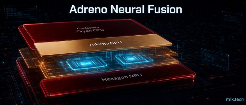
The GPU reveal on 2 September carried the generation’s only genuinely new block of silicon. Adreno Matrix Cores put AI-dedicated units inside the graphics pipeline for the first time, which Qualcomm correctly calls a first for Adreno and carefully never calls a first for mobile. Apple put neural accelerators in every GPU core of the A19 Pro a year ago, and Arm’s NX neural accelerators are shipping right now inside the Mali-G2 Ultra NX. Qualcomm arrives on the same calendar as Arm’s licensees, a year after Apple, having spent the previous year explaining that Hexagon was where the AI lived.
Vendors converged here for architectural reasons, not fashion. A neural upscaler is a small network that runs every frame, between render and display, on data already sitting in GPU memory. Run it on shaders, and you hand back a chunk of the win you were chasing by rendering at lower resolution in the first place. Run it on the NPU, and you copy the frame out of the graphics subsystem, across the fabric, and back, which costs latency you cannot hide and DRAM bandwidth you cannot spare. A matrix unit inside the GPU is the only design that does not lose on either axis. Nvidia worked that out in 2018. Mobile took eight years to follow, and it followed in the year DRAM got expensive.
The memory number attached to it is the part I keep pushing back on. Eighteen megabytes of Adreno High Performance Memory is presented as part of the new pitch, and it is the exact capacity Gen 5 has been shipping since the Xiaomi 17 landed last October, same three-slice layout. Qualcomm did not add a byte of GPU cache. Worse, the leak tables suggest 18MB only applies to the Extreme tier with its Adreno 850; the standard part’s Adreno 845 is listed at 12MB, which would make the GPU memory story a reduction for most buyers rather than a hold. If that survives the Summit, the 18MB figure is doing double duty as a headline and a tier gate.
What Qualcomm gave on the GPU is a 40 percent power saving with Neural Fusion enabled, quoted in briefing material rather than the blog, against a previous solution nobody has defined. Super resolution on shaders, Frame Motion Engine, or native rendering at output resolution are three entirely different baselines, and the claim means three different things depending on which it is. The whole-GPU efficiency figure is 12 percent, on a clock that moved from 1.2GHz to 1.45GHz, which on a node transition of this size means most of the budget went into frequency and the new units rather than being banked.
The strongest concrete thing in the GPU post is distribution, not performance. Unity and Unreal are integrated, and Qualcomm calls the technology commercially available, meaning the SDK is in studios’ hands rather than in a game you can download today. The unanswered question is the fallback: Arm ships one plugin that runs NSS on NX hardware and drops to ASR everywhere else, and says so plainly. Qualcomm’s post does not say whether Neural Fusion degrades to a shader path, falls back to the older super resolution, or simply switches off on every Adreno without Matrix Cores. For a studio deciding whether to ship the integration, the fallback story matters more than the flagship story, because the flagship is a rounding error in the install base for the first eighteen months.
The NPU is the one that gave numbers
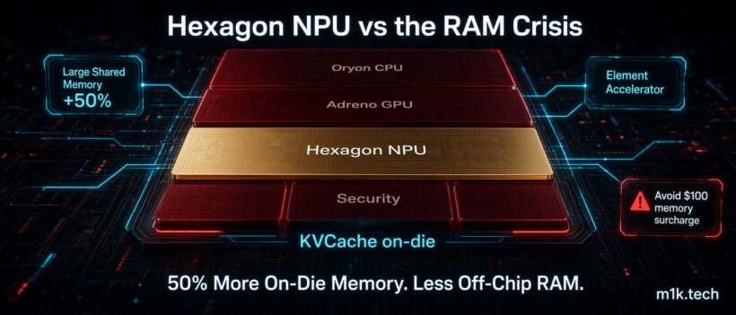
The Hexagon post on 10 September is the most specific of the three, and its specificity tells you the most about the strategy. I read it as Qualcomm’s answer to the RAM crisis, and rereading it against the other two only strengthens that.
Two things are new. An Element Accelerator is purpose-built for transformer workloads and sits alongside the existing scalar, vector, and matrix extensions rather than replacing them. The shared memory subsystem also grows by 50 percent, so more model state, activations, and intermediate tensors stay on-chip instead of going out to DDR. Vinesh Sukumar, who wrote the post, runs AI and generative AI product management, and the framing is his department’s rather than a marketing team’s: agents are a system of specialized models routed by task and context, not one large model answering everything.
The model architecture claim is the one worth sitting with. Qualcomm says a 30-billion-parameter Mixture-of-Experts model can keep tens of billions of parameters available while activating only about 3 billion routed parameters per token generation step. Combined with what it calls flash-to-memory expert management and caching, that describes a phone running a model far larger than its DRAM could hold by keeping most experts in storage and pulling in only the ones the router picks. Precision support spans INT2, INT4, INT8, FP8 and FP16. For INT4 models, prefill improves by up to 50 percent, with faster decode, enhanced speculative decoding, and higher tokens per second.
This has been Qualcomm AI Research’s published position for a while, which is why I believe the hardware follows it. Their cache-conditional mixture-of-experts paper attacks precisely this problem in software: on a phone that cannot hold every expert in DRAM, you condition the router on what is already cached so the model preferentially picks experts you can reach cheaply. They demonstrated it on Qwen-MoE running on Snapdragon hardware at INT4 and INT8, and the throughput gain over a plain least-recently-used cache was substantial. The Element Accelerator and the bigger shared pool are the hardware end of that same idea. Given that most frontier releases have gone MoE, and that the whole family is memory-bound rather than compute-bound during decode, a company betting its 2027 mobile story on on-device agents has no choice but to attack the memory path.
What Qualcomm still lacks is its own model. AI Hub is a catalog of other people’s weights compiled down to Hexagon, and the in-house contribution is the runtime, the quantization, and the routing research. I think that is the right division of labor for a silicon vendor, and I also think it means Qualcomm’s AI story stays hostage to whatever Alibaba, Google, and Meta decide to open-weight next. One CPU-side question also remains open. Oryon Gen 3 moved to Armv9-A with SVE2 and SME1, the first Scalable Matrix Extension. Arm’s Lumex C1 cores shipped SME2, and MediaTek’s new flagship uses the C2 generation. If Oryon Gen 4 is still on SME1, Qualcomm is a matrix-extension generation behind on the CPU while leading on frequency, and the workloads where that shows up are exactly the small on-CPU inference tasks agentic loops fire constantly. No leak has settled it.
Cache as a memory-price hedge
Now the part that ties the three posts into one decision.
The mobile DRAM market has come apart this year. LPDDR5X contract prices rose 58 to 63 percent quarter over quarter in Q1 2026, then TrendForce put Q2 growth at 93 to 98 percent on top of that. Memory has gone from 10 to 15 percent of a smartphone bill of materials to somewhere between 30 and 40 percent. Counterpoint has flagship BOM up 100 to 150 dollars in Q2 alone and expects 150 to 200 dollars at retail. By Q1, 16GB of LPDDR5X plus a terabyte of UFS 4.1 crossed 280 dollars per device, more than the Snapdragon 8 Elite Gen 5 costs. The memory now costs more than the processor. I have watched that number reach actual retail prices on Samsung’s foldables, kill an entire Nothing sub-brand device outright, and push the Poco F9 Ultra into reusing last year’s chipset.
TrendForce’s read is that flagships slide from 16GB to 12GB and budget phones from 8GB to 4GB. IDC has DRAM supply growth at 16 percent for the year, below historical norms, because every wafer that goes to an HBM stack for an Nvidia part is a wafer that does not become LPDDR5X.
Against that backdrop, three separate memory claims in three separate posts stop being a coincidence and start being a product-planning position. If your OEM customers are about to ship phones with less RAM than last year’s, silicon that tolerates less RAM gracefully is worth real money. Qualcomm is selling SRAM as a partial substitute for DRAM it cannot make its customers afford: on the CPU through a shared pool, on the GPU through a local one, and on the NPU through both a bigger pool and a model architecture that needs less of what it does not have.
The catch is that SRAM has not scaled meaningfully in years. Logic keeps shrinking; cache cells mostly do not, so a bigger on-die pool on a node whose wafers reportedly run around 30,000 dollars against 18,000 to 20,000 for 3nm is one of the most expensive ways to buy your way out of a memory problem. That is probably part of why the CPU’s L2 total went down rather than up, why the GPU pool did not grow at all, and why this generation splits into two price tiers instead of one.
MediaTek launched first and landed lower
The thing I was watching for in August happened on 15 September, and it split two ways.
MediaTek announced the Dimensity 9600 Pro in Hsinchu a week before the Summit and took the 2nm milestone off the table. That is the calendar claim Qualcomm lost, and MediaTek will get to keep it. But the clock claim went the other way, further than I expected. The 9600 Pro is 2+3+3 on N2P with over 33 billion transistors: two Arm C2-Ultra cores at 4.55GHz, three C2-Pro at 4.35GHz, three more C2-Pro at 3.10GHz. Every pre-launch leak had those Ultra cores near 5.0GHz. They landed at 4.55. Qualcomm’s first-mobile-CPU-to-5GHz line survives, and it survives on merit rather than on timing.
The cache comparison is the one that should worry San Diego. MediaTek shipped 34.5MB of total cache: 8.5MB of L2, a real 16MB L3, and 10MB of system-level cache. Set that against Qualcomm’s leaked 16MB shared L2 plus 6 to 8MB of SLC, and the two companies have answered the same question in opposite directions. MediaTek’s answer to the memory wall is more cache and a proper mid-level tier. Qualcomm’s is less cache, allocated smarter. One is an architectural bet, and the other is a capacity purchase, and only one depends on an allocation policy working as advertised under a real Android scheduler.
The AI convergence is almost comic. MediaTek’s NPU 1090 claims 51 percent higher LLM prefill and 55 percent more tokens per watt. Qualcomm claims up to 50 percent higher prefill on INT4. MediaTek puts its on-device model ceiling at 30 billion parameters. Qualcomm’s headline MoE example is 30 billion parameters. Both ship LPDDR6 support and UFS 5.0 on the top tier. Both have now put neural units inside the GPU: MediaTek via Arm’s 12-core Mali-G2 Ultra NX, with a 27 percent performance gain at 24 percent lower power. When two competitors independently arrive at the same three numbers in the same month, the numbers are describing the constraint rather than the cleverness.
MediaTek is also better funded for this fight than ever. It raised 3.9 billion dollars through a convertible bond in August, with Nvidia putting in 3.5 billion of it and Alphabet participating. First phones are the vivo X500 series on 21 September, one day before Qualcomm takes the stage, followed by the Oppo Find X10 Pro Max.
Apple answered differently again. Apple announced the iPhone 18 Pro and Pro Max on 9 September with the A20 Pro, and reporting on its node is genuinely inconsistent, with outlets splitting between a 2nm-class part and a 3nm-class one. The packaging is not in dispute: Apple pairs the SoC and DRAM in a wafer-level multi-chip module with no interposer. Qualcomm keeps more data on-die; Apple shortens the trip to the data that will not fit. Both are admitting the memory interface is the wall.
Samsung’s Exynos 2700 on SF2P remains the outlier. Internal Samsung testing reportedly has it 19 percent ahead of the Snapdragon 8 Elite Gen 6 in multi-core and 9.5 percent ahead of the higher-binned part, with a 22 to 24 percent GPU lead at a 2.5W cap. Those numbers came from Samsung, ran through Yonhap, and nobody with silicon in hand has reproduced them. Samsung Foundry’s SF2 comeback is the real story underneath them regardless of whether the benchmark holds, and it has a direct commercial edge for Qualcomm: Samsung’s yields cleared 70 percent and Qualcomm still will not pay the asking price, which is why those talks have reportedly slid into 2027.
Then there is Xiaomi, which shipped the argument before anyone else got to make it. The Xring O3 is a ten-core, all-big-core design with 60MB of on-chip cache, including a 16MB system-level cache, the industry’s first LPDDR6 controller at 113.8 GB/s, and 82ns memory latency. Xiaomi could only delete its efficiency cores because it fed the big ones properly. Same thesis as Flex Cache, executed through raw bandwidth and capacity rather than allocation policy, and it shipped in the Xiaomi 18 Fold on 7 September rather than in 2027.
What the Summit has to sell into
Qualcomm walks into Maui from a weaker position than the engineering suggests, and the two-tier product plan is the tell.
Fiscal Q3 closed in June with 9.95 billion in revenue, at the high end of guidance, and non-GAAP EPS of 2.21, which missed. Handset revenue fell 20 percent year over year to 5.09 billion, and management named memory dynamics explicitly: OEMs cut chipset purchases and worked down inventory because their own memory bills exploded. So the RAM crisis is not just something Qualcomm’s chips are designed around; it already showed up in Qualcomm’s own revenue line. Automotive was the bright spot at 1.59 billion and 61 percent growth, its twenty-third consecutive quarter of double-digit gains. The stock fell 7 percent anyway.
The Apple line is what moved it. Modem share in the next iPhone launch is now expected materially below the prior 20 percent estimate, with Apple product revenue down roughly 50 percent sequentially into the December quarter. That was always coming, and I have been writing about the expiration date on that relationship for a while, but it is arriving in the same twelve months as the memory squeeze.
Chip prices went up on 1 September, three weeks before the Summit, to cover wafer, memory, assembly and packaging inflation. So the sequence reads: raise prices, announce a chip on a wafer that costs 30 percent more, split it into two tiers so the expensive one only lands where buyers tolerate it, and pitch the memory architecture as the thing that keeps performance intact when your customers ship less RAM. Every piece of that fits together. It is a coherent response to a bad year, and it is not the response of a company with pricing power to spare.
Who gets it first
Two part numbers are in circulation: SM8950 for the standard chip and SM8975 for the higher tier. Digital Chat Station has the retail names as Snapdragon 8 Elite Gen 6 and Snapdragon 8 Elite Extreme Gen 6, which drops the widely-assumed Pro branding and lines the mobile family up with the X2 Elite and X2 Elite Extreme on the PC side. Qualcomm teased two chips on 19 August with the phrase “When Two Changes the Game,” and has since confirmed a dual-flagship launch outright.
Xiaomi is the anchor. The company confirmed earlier this year that the Xiaomi 18 and 18 Pro Max run Qualcomm’s next flagship, with the 18 Pro Max and a rumored 18 Ultra taking the SM8975. The Xiaomi 18 Fold went the other way at IFA on 7 September with the in-house Xring O3, a useful reminder that Qualcomm’s supply agreement still covers the global flagships while the Xring accumulates leverage underneath it.
Beyond Xiaomi, the Extreme part shows up in leak clusters around the Galaxy S27 Ultra, the vivo X500 Pro Max, the OnePlus 16, and the Oppo Find X10 Ultra. OnePlus taking the Extreme in a device that is not an Ultra is the aggressive choice in that list, and it suggests how OnePlus wants to be perceived after the 15R made the cheaper Snapdragon look like the smart buy. iQOO 16, Redmi K100 Pro Max and Galaxy Z Fold 8 appear in the same reporting.
Vivo is the interesting case, because it is taking both. The X500 series launches on 21 September with MediaTek’s 9600 Pro, and the X500 Pro Max has been appearing in benchmark databases with the SM8975. That’s vendor hedging within a single product line in the same quarter, which happens when neither chip has a decisive lead and both suppliers are negotiating hard.
Samsung’s split looks like this year’s: Galaxy S27 and S27+ get Exynos 2700 everywhere except the US, Canada, China and Japan, with the S27 Ultra on Snapdragon globally, as the S26 Ultra was. If the Exynos numbers survive independent testing, that split gets renegotiated for the S28 rather than the S27.
The longer bet
None of this is where Qualcomm thinks its future revenue comes from, and it has stopped pretending otherwise.
Management doubled the fiscal 2029 non-handset target from 22 billion to 40 billion. It closed the Modular acquisition, reported at around 3.1 billion dollars, to buy a compiler stack that runs models across architectures without hardware-specific rewrites, which is a bet against CUDA rather than a bet on phones. It stood up the Dragonfly data center line with Meta signed, then added Amazon on a deal worth up to 60 billion dollars, sweetened with a 4 billion dollar stock warrant. Data center silicon is supposed to start generating revenue in the December quarter, against a 15 billion dollar target by 2029.
Read the mobile platform through that lens and the agentic framing stops looking like a marketing coat of paint. The same architectural moves show up at both ends of the company: put the compute next to the memory, keep the working set local, and choose model architectures that let you get away with less bandwidth. An NPU that runs a 30B MoE by activating 3B parameters per token is doing on a handset exactly what Qualcomm’s inference racks are designed to do in a rack, which is compete on cost per token rather than on peak throughput. I mapped the full strategy in August, and this is the mobile chapter of it, not a separate story.
Which leaves the thing I will actually be checking on the 22nd. The most quotable number in this whole three-post sequence is the least informative: 5GHz on its own is a binning outcome on a node Apple and MediaTek are also buying, and the IPC claim standing next to it still has no number attached. The real decisions are the Flex Cache capacity and the policy that divides it, whether the GPU pool holds at 18MB or drops to 12 on the tier most people will buy, and whether the NPU’s MoE story survives contact with a model somebody else trained. If Qualcomm opens with gigahertz instead of megabytes, that will tell me megabytes aren’t the story they want told.
Sources
- Qualcomm, The Qualcomm Oryon CPU is the first mobile CPU to reach 5GHz, OnQ blog, 25 August 2026
- Qualcomm, Qualcomm Adreno Neural Fusion breaks the AI-graphics tradeoff with new hardware accelerator, OnQ blog, 2 September 2026
- Qualcomm, Why agentic AI needs a completely different mobile architecture: the Qualcomm Hexagon NPU, OnQ blog, 10 September 2026
- Qualcomm, Snapdragon Summit 2026, 22-24 September 2026
- Qualcomm AI Research, Mixture of Cache-Conditional Experts for Efficient Mobile Device Inference
- Beebom, MediaTek Dimensity 9600 Pro: benchmarks and specs
- CNET, MediaTek’s Dimensity 9600 Pro focuses on gaming, AI performance for high-end phones, 15 September 2026
- Hardware Busters, Qualcomm drops Matrix Cores into the Adreno GPU, and the Snapdragon 8 Elite Gen 6 hits 5GHz
- TechTimes, Snapdragon 8 Elite Extreme Gen 6 hits 5.11GHz in Geekbench 7 before Qualcomm reveal, 10 September 2026
- Notebookcheck, Qualcomm Snapdragon 8 Elite Gen 5 benchmarks and specs
- TechInsights, Snapdragon 8 Gen 5 Duo powered by Oryon with SME1
- Chips and Cheese, Qualcomm’s Oryon Core: a long time in the making
- GSMArena, Even more details about the Snapdragon 8 Elite Gen 6 leak
- IDC, Global memory shortage crisis: market analysis and impact on smartphones and PCs in 2026
- Qualcomm fiscal Q3 2026 earnings call, highlights and guidance
- Android Central, Qualcomm teases dual 8 Elite chips for Snapdragon Summit
- Android Headlines, Snapdragon 8 Elite Extreme Gen 6 naming
- SamMobile, More details about Samsung Galaxy S27’s Snapdragon 8 Elite Gen 6 chip
- 9to5Mac, iPhone 18 Pro’s A20 chip and WMCM packaging