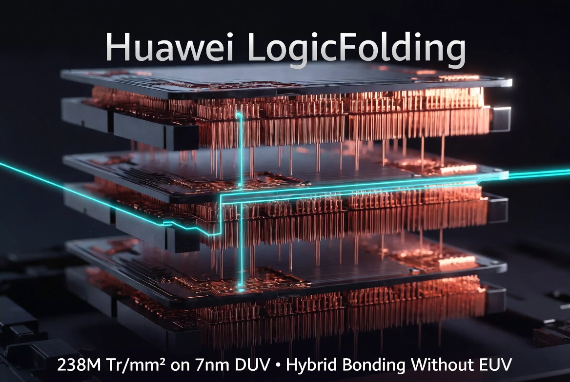
Huawei’s LogicFolding architecture uses hybrid bonding at a 1.5 µm interconnect pitch to achieve a claimed system-level transistor density of 238 million per square millimeter on SMIC’s 7nm DUV process. That pitch is 16 to 36 times denser than current offerings from TSMC and Intel, and underpins the Kirin 2026 chip.
Rather than relying on lithographic shrinks blocked by export controls on EUV equipment, Huawei treats the bonding interface as the primary scaling lever, stacking CPU, GPU, NPU, and memory dies vertically to reduce signal path lengths and energy per bit. The claimed density figure is a system-level metric, not a per-die one, and independent verification of yields and real-world performance has not yet been published.
238 million transistors per square millimeter, built on a 7nm DUV process with no EUV in the building. That is the number He Tingbo put on stage at ISCAS 2026 in Shanghai, and it lands in the same tier as TSMC’s N3. He runs HiSilicon and chairs Huawei’s Scientist Committee, and the paper he presented lays out the 3D stacking architecture under the coming Kirin 2026. The trick is hybrid bonding at a 1.5 µm interconnect pitch.
Conventional 3D packaging leans on copper bumps, little solder-like protrusions that press together to make electrical contact between stacked dies, and pitch is where they hit a wall. Microbump technology has stalled around 10 µm, so you get roughly one interconnect every 10 micrometers along the bonding interface, and that ceiling caps how much bandwidth and how many signal paths you can push between layers.
Hybrid bonding throws the bump out. Copper pads sit flush with a dielectric (usually silicon oxide or nitride) on the face of each die. Bring two prepared surfaces together, heat them, and the copper expands and diffuses across the seam into a direct metal-to-metal bond, while the dielectric fuses to its counterpart to provide mechanical strength. The interface is now planar and bump-free, and pitch is set by how finely you can lithographically pattern the copper pads rather than by the physics of forming a bump. The catch is alignment: the bonding tool has to place dies with precision measured in tens to hundreds of nanometers. Clear that bar and interconnect density scales with lithography instead of bump metallurgy.
Shorter, thinner copper has lower resistance and parasitic capacitance than a bump, so energy per bit drops and signal integrity improves. If you are a designer shoving huge volumes of data between a CPU cluster, a GPU, an NPU, and DRAM sitting on separate dies, that is the whole game.
1.5 µm sits so far outside the mainstream that the industry map is the fastest way to feel it. TSMC’s SoIC platform, the packaging behind Apple’s M-series, runs at roughly 6 µm today and has reportedly targeted about 4.5 µm around 2030. Intel’s Foveros Direct, shipping in Clearwater Forest this year, sits at 9 µm. SemiAnalysis, which published the comparison, pegs Huawei’s 1.5 µm at 16 to 36 times denser in interconnect count than the leaders, depending on which one you compare it to. The math is unforgiving because density scales with the inverse square of pitch: 6 µm down to 1.5 µm is a 4× pitch reduction and therefore 16× the interconnects per unit area, and against Intel’s 9 µm it stretches to 36×. That is not a tuning improvement. It is a different regime of inter-die communication.
Huawei’s paper names 1.0 µm for the 2027 Kirin generation and sets a 2031 goal of transistor density equivalent to a 1.4 nm-class node, achieved through continued system-level scaling. That 2031 target trails TSMC’s projected native 1.4nm physical node by about three years, but the route there is nothing like TSMC’s.
Huawei calls the architecture LogicFolding. Instead of cramming CPU, GPU, NPU, and memory onto a single monolithic die or wiring them through a conventional interposer, it stacks those blocks vertically across the hybrid-bonding interface. Data between the NPU and its memory then travels only micrometers through a bond rather than millimeters across a package substrate or a PCB trace, so the resistive and capacitive loads drop proportionally, energy per bit falls, and sustainable bandwidth rises. Splitting a design across multiple stacked dies buys floorplanning freedom too. Each die is optimized on its own, and a critical path that would otherwise snake around unrelated logic can be shortened. He Tingbo folds all of this into what the paper calls the Tau (τ) scaling law, described internally as “He’s Law,” which swaps Moore’s transistors-per-area metric for a system-level one built on signal propagation latency across the whole device hierarchy. The claim is that compute performance and efficiency come down to how fast signals cross circuits and systems, not how tightly transistors pack onto a single die, and that shrinking propagation time by architecture can stand in for a lithographic shrink or ride alongside one. Huawei says 381 distinct chips have gone into mass production over six years on early variants of this architecture, which puts the origins around 2020 and several product generations of refinement before Kirin 2026.
Read the 238 MTr/mm² figure carefully, because it is not the number it looks like. TSMC’s N3 achieves comparable density on a monolithic die, with 238 million transistors in a single square millimeter of silicon using a single lithographic process. Huawei’s number is system-level effective density: total transistor count of the stacked assembly divided by its footprint. Treating the two as the same thing hides the engineering tradeoffs.
Heat is the first of them. A buried die has to push its heat through bonding interfaces and overlying silicon before it ever reaches a spreader, and the interface conductivity, the die thicknesses, and the power density of each block all fight each other. Samsung’s Exynos 2700 dodges the problem by keeping DRAM physically separate and running a copper Heat Pass Block, precisely because jamming high-power logic and DRAM into a tight vertical stack cooks. Apple’s A20 Pro attacks the same heat from another angle with a Wafer-Level Multi-Chip Module and direct vapor chamber contact.
Yield is the other exposure. A monolithic die works or it does not; a stack multiplies its odds. Four dies at 95% yield each land the assembly near 81% before you count a single bonding defect, and at 1.5 µm the alignment and bonding step adds failure modes of its own. Nobody outside Huawei has confirmed those yields at production scale. The ISCAS paper is Huawei’s own telling, and no third-party teardown of Kirin 2026 exists yet. TechInsights has cracked open Kirin silicon before and is the likeliest source for an independent density read.
None of this is separable from the sanctions. ASML’s EUV systems are blocked from China under U.S. and Dutch export controls, which leaves SMIC on DUV with its most advanced node around 7nm-class. Buying a better node, the normal path to more density, is simply shut. So Huawei made the bonding interface itself the primary scaling lever instead of treating packaging as a way to bolt together chips built elsewhere. Hitting 1.5 µm is a genuine feat if the claims hold, demanding extremely precise wafer prep, copper pad patterning below 2 µm, and bonding gear that aligns to sub-100 nm. CEA-Leti and Imec have shown sub-micrometer wafer-to-wafer hybrid bonding in the lab, per IEEE ECTC 2026, but volume production at these pitches is another animal entirely.
Call it leadership or call it a clever reframing of a boxed-in position, and the answer is both. On interconnect pitch alone, Huawei is ahead of TSMC and Intel by a wide margin, engineering around a wall its rivals never hit. Kirin 2026 will not match the raw per-transistor performance of N3 or N2 parts, because SMIC’s DUV transistors are simply less advanced, and Huawei’s whole bet is that system-level efficiency and effective density paper over that gap. That is the claim I doubt survives independent benchmarking, and until it does, the Tau framework stays a fascinating pitch rather than a proven alternative to node-based roadmaps.